

On the other hand, established component sizes continue to be used. In the automotive sector, in particular, large components, such as certain types of connectors, are the backbone of enduring industry standards that are passed down through generations. Consequently, the range and variety of component sizes that the machine must handle is constantly increasing.
The production of multilayer boards is more affordable than ever, and their use is growing as designers employ every feasible measure to miniaturize product dimensions. Surface-mount components are becoming increasingly spaced, which presents greater lighting challenges, such as shadows.
Furthermore, as assembly complexity increases, each board presents more features that must be inspected. To address this, inspection algorithms can be improved and optimized to leverage the performance gains that come with the latest processing engines. The introduction of AI into these processing engines is an exciting new development that can dramatically improve and accelerate anomaly detection.
Furthermore, improvements that facilitate the use of AOI equipment are important for helping to increase program accuracy and productivity.
Overcoming Historical Obstacles
: To ensure that image quality remains sharp as component sizes become increasingly smaller, it is important to ensure that lighting, camera resolution, and lens characteristics are optimized. In the latest YRi-V 3D AOI system, Yamaha combines a 12MP camera with an enhanced 5µm lens option (Figure 1), in addition to 12µm and 7µm lenses. When inspecting surface mount assemblies at high speed, the high-resolution lens facilitates the inspection of even the smallest parts, down to the size of an SMD 0201 chip. It works in conjunction with the YRi-V's new coaxial illumination system, which is specifically designed to help find minute defects. This coaxial light can be configured for use in automated routines down to the single-step inspection level, enabling the YRi-V to identify defects such as scratches and cracks in components such as wafer-level chip-scale encapsulated (WLCSP) components that have a shiny, reflective surface.
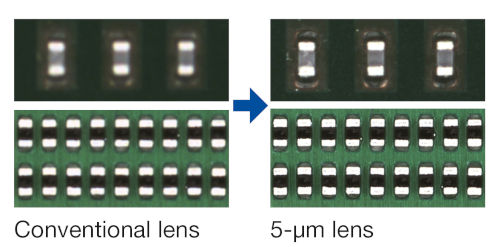 Figure 1. The high-resolution lens allows for the clear capture of minute details.
In addition to the higher resolution of the 5 µm lens, the image processing subsystem has been enhanced with the latest generation graphics processing unit (GPU) chips. This has accelerated the inspection cycle time by 60–100%. The combined effect of the improved lens and processing technology provides a simultaneous increase in inspection resolution and throughput.
However, smaller component sizes are just one aspect of the challenges posed by the latest board designs. As board designers take advantage of affordable multilayer manufacturing to pack more features onto smaller printed circuit boards, components are being spaced further apart on the board surface with each successive generation of products.
While multilayer boards offer exciting new opportunities for designers, they also present a challenge for inspection. In particular, small components, such as SMD chips, can create blind spots when placed next to larger parts, obstructing a clear view of the larger component's I/O pins and associated solder pads. Conversely, larger parts can cast shadows on smaller components, such as SMD chips placed between them, preventing the assessment of solder terminations and any surface markings and polarity.
New features, including an 8-way projector (Figure 2), available with the Yamaha YRi-V system, now effectively overcome these problems. The maximum measuring distance has also been extended to 25 mm. The improved projector eliminates shadows by ensuring uniform illumination of all elements within the field of view. The expanded measuring capability allows for close inspection while handling a wide range of component sizes, from the smallest to the largest.
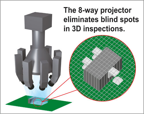 Figure 2. Enhanced lighting eliminates shadows and blind spots.
AI-Enhanced AOI
While the machine’s next-generation GPU performance has enabled faster image processing and defect detection, artificial intelligence (AI), or machine learning, is poised to bring game-changing new capabilities to AOI, just as it has in many other aspects of industrial and consumer technology.
Leading the trend, Yamaha’s YRi-V system has introduced important new AI-based skills to help simplify equipment setup and operation. These include automatic component library matching, which uses deep learning to identify component types from images and thus enable automatic selection of the optimal component library. In addition, AI is used to assist with 3D component measurement to generate data for components not found in any existing library. Finally, AI is used to analyze captured images and help determine their accuracy. This combines a machine-based element of certainty with the flexibility of human visual inspection, resulting in a fast, accurate, and repeatable pass/fail judgment.
Four-Angle Inspection and Algorithms
: Historically, solder defects are the most difficult for AOI systems to analyze. Some, such as head-in-pillow defects that occur when solder fails to wet against the component's termination, are notoriously difficult to detect using conventional equipment and approaches. Solder bridges can also be difficult to identify with certainty.
Yamaha's four-angle inspection cameras have helped overcome these challenges by capturing images from oblique angles, allowing the system to capture a complete picture of each inspection location. The YRi-V upgrades these cameras with a 20-megapixel resolution to capture finer details. In combination with the camera upgrade, improved 4D inspection algorithms leverage the increased image information to enhance the detection of issues such as bridges and head-in-pillow defects.
Program and Software Generation:
Some AOI systems offer optimal performance when installed in-line with other equipment running the same software platform. A more open approach, such as the one adopted by Yamaha, allows users to unleash the full potential of their AOI system by working with any type of equipment on the line. In particular, rapid program generation is possible using Yamaha's YSUP software, which is open-source and license-free.
The comprehensive YSUP software can convert inspection data directly from CAD/CAM or YGX and also supports Gerber data as standard. Furthermore, the YSUP functionality of the YRi-V offline programming software can create AOI programs from ODB++ data without requiring a YGX file. If the PCB template is present in the ODB++ data, it can be imported as a simplified image to aid in positioning new components using the offline programming station. This eliminates the need for programmers to take control of the factory's AOI system to scan the PCB and create a template image, thus avoiding disruption to normal production.
The software automatically generates and displays virtual images of the production printed circuit board without requiring any special expertise. Other automated features include the detection of any through-hole components, with the ability to generate appropriate inspection data. New features also allow for data adjustments, such as automatic detection of inspection areas based on component shapes and pad positions. This increases convenience and eliminates the need for inspection frames. Furthermore, the software automatically determines lighting parameter settings to ensure optimal illumination, minimizing trial and error and reliance on user experience. Automatic position correction, based on the amount of component misalignment, further minimizes operator intervention. Together, these features can reduce data setup times by up to 50%.
Conclusion:
Today's leading electronics assemblers need an Applied Optical Image (AOI) system to help them continue improving productivity. Solutions are needed for perennial challenges, such as defects that are difficult to identify. Furthermore, the latest AOI systems must also address the challenges presented by new technologies, such as densely populated multilayer boards.
The latest image processing technologies, as well as cutting-edge techniques like machine learning, are now needed to enhance defect detection and accelerate image analysis and programming. The new generation of AOI systems entering the market also introduces superior multi-angle illumination, higher image resolution, and user-friendly software for setup and management, equipping owners for the challenges ahead.