


In many embedded systems applications, discrete logic devices, such as the 74HC series, are commonly used. The advantage of these logic devices is that they operate independently of the microcontroller and can respond much faster than software. However, these devices add to the bill of materials and require more space on the printed circuit board.
To address this issue, many Microchip microcontrollers incorporate a peripheral called a CLC (Configurable Logic Cell) in PIC® microcontrollers or a similar peripheral called a CCL (Configurable Custom Logic) in AVR® microcontrollers. Both peripherals implement custom, software-defined logic that can be executed independently of the CPU. In other words, once the custom logic function is configured, its operation is independent of the microcontroller.
However, a limitation of these peripherals is the small amount of logic they offer. Each CLC is roughly equivalent to a single look-up table (LUT), while each CCL integrates a pair of independent LUTs. These peripherals are powerful tools for developing simple logic circuits. They combine signals and integrate with other hardware peripherals. For example, all the examples of debounce on a hardware button, generation with the WS2812 , and quadrature decoding require these peripherals, but there are only a few of them on the microcontroller, which limits the complexity of the applications.
a Configurable Logic Block (CLB) , was added to the PIC16F13145 microcontroller family, as shown in Figure 1. Note that the CLB does not replace the CLC or CCL peripherals, and the devices can be one or more CLC/CCLs or a CLB.

Figure 1. CLB Block Diagram.
The PIC16F13145 family's CLB consists of four sets of Logic Groups, each containing eight BLEs. The BLEs in each logic group are connected; each group represents two GPIO outputs and an optional CPU interrupt. When operating at 5.5V, the BLEs have a typical propagation delay of less than 6 ns. All BLEs share the same clock structure, the source of which is configured in software along with an optional clock divider. The CLB can use one of the microcontroller's internal clock sources or an external source.
The peripheral is initialized from the microcontroller's memory and can control the pins directly from the structure itself via Peripheral Pin Select (PPS). PPS allows the user to reassign I/O pins used by hardware peripherals, greatly increasing design flexibility. For example, if RA1 was used for the SPI Clock, it would be more advantageous to use RA6, and PPS would reassign the pin.
Other elements integrated into the CLB include a 3-bit hardware timer with decoded outputs, an edge detector for input signals, and a 32-bit output register for debugging. Other outputs from the microcontroller's Core Independent Peripherals (CIPs) can be used as inputs to the CLB in more complex designs.
Because the CLB is considerably more complex than the CLC or CCL, a new tool called CLB Synthesizer has been developed. CLB Synthesizer provides a graphical interface for configuring the logic, as shown in Figure 2. In addition to primitive logic, the tool also supports higher-level logic blocks, which can be supplied or custom-built by the user.
Interacting with the graphical tool generates a Verilog module in the background for synthesis. If the developer prefers to write their own Verilog, or has a prepared file, it can be imported directly into the tool as a module.
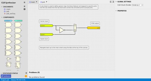
Figure 2. CLB Synthesizer with a PSK (Phase-Shift Keying) example.
The output of the CLB Synthesizer is an assembler file containing the bitstream for adjusting the CLB and source code for configuring the CLB as a peripheral. This tool can be run through MPLAB® Code Configurator (MCC) or a online tool . MCC is a code generation utility that allows users to adjust and configure peripherals on the microcontroller through a visual interface. After configuring the hardware peripherals, MCC generates the initialization code and a device API.
During runtime, the CLB bitstream is loaded directly from program memory using the onboard hardware. One advantage of this solution is that you only need to change the CLB configuration while the program is running, and the loading process can be repeated with a different bitstream stored in the device memory.
A series of usage examples have been created to demonstrate the CLB's functionality in applications. Let's look at two examples: the 7-segment display converter and the SPI to WS2812converter. These examples are functional blocks that can be copied and used as part of a complete solution. They were developed to demonstrate the usefulness of this peripheral and what it can contribute to a design.
The first example is a 7-segment display converter. 7-segment displays can be controlled from normal I/O pins, but a standard implementation usually requires a software-defined lookup table to convert the input number into the correct output pattern for the display. In this implementation, the CLB functions as a hardware lookup table. The desired output character (0 to F) is loaded into the CLB's input register from the software. Each output segment of the display is controlled by a LUT that maps inputs and outputs.
This example was used internally to build a new control board for the synchronization system. The original user interface was developed in the 1980s using 74HC series logic. With the CLB, a single 20-pin microcontroller can implement the display and keypad logic on the board, thus significantly reducing the bill of materials. Figure 3 compares both technologies.
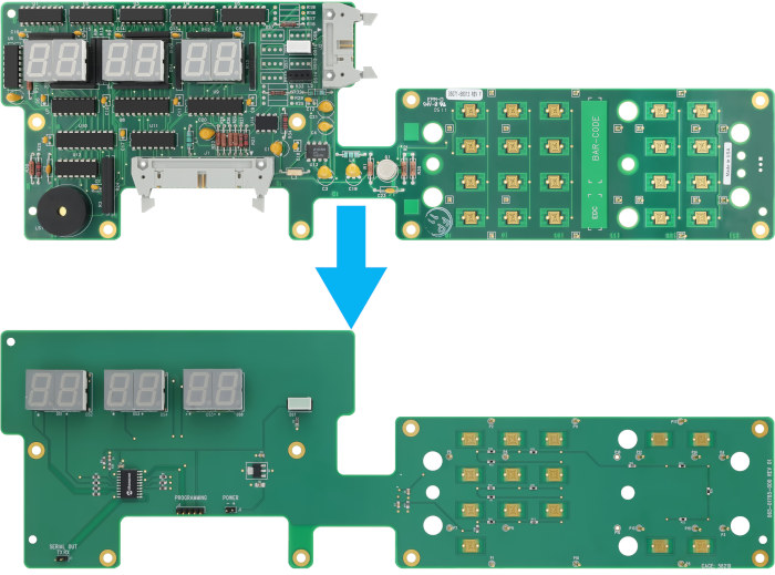
Figure 3. Comparison between the original printed circuit board and the new assembly. This example was developed by Josh Booth.
The SPI-to-WS2812 converter is shown below . The WS2812 is a single-wire serial protocol for controlling LED matrices using pulse-width modulation. In this case, the SPI hardware is used as a shift register for the data sent to the LEDs, while the CLB converts SCLK and SDO to the intended output.
This is implemented in the example using a 3-bit single-shot counter, a D latch with Enable, and a 4-input LUT, as shown in Figure 4. The key to this solution lies in the clock sources for SPI and CLB. The SPI clock is held high in standby mode, changes state on a rising edge, and operates at the WS2812 output frequency (800 kHz), while the CLB clock source is ten times that speed (8 MHz). When SCLK goes low, the 3-bit counter starts counting. When the counter reaches 7 (0b111), it stops and remains at 0 until the next low period of the clock pulse.
The counter's output is fed into a 4-input LUT along with a retained version of the output data. This establishes the data output pattern, which can be seen on the right side of Figure 4. Once the counter is reset, its output will follow 0 to complete the cycle. Then, if necessary, the next byte is transmitted on the hardware SPI, and the cycle repeats.

Figure 4. Block diagram of the SPI to WS2812 converter developed by Petre Teodor-Emilian.
Both examples demonstrate the advantage of integrating discrete logic into a microcontroller. Hardware peripherals offload tasks from the CPU, which can improve response time and power consumption, as well as reduce the number of components. The CLB allows the development of complex applications that were previously impossible to implement on a microcontroller. Currently, the CLB can be found in the PIC16F13145 microcontroller family, available through Microchip Direct or other distributors.
Author: Robert Perkel, Applications Engineer in the 8-bit Microcontrollers Business Unit, Microchip Technology
Robert Perkel is an Applications Engineer at Microchip Technology who develops technical content such as application notes, articles, and videos. He is also responsible for analyzing peripheral use cases and developing code samples and demonstrations. Perkel studied at Virginia Tech, where he earned a degree in Computer Engineering