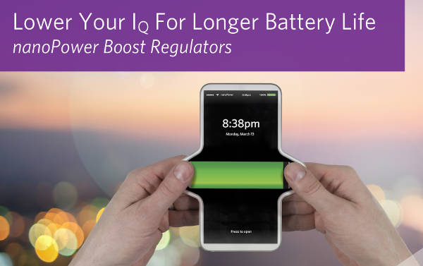
Designers of wearables, IoT devices, mobile devices, and other connected devices are struggling to extend battery life for next-generation products, particularly with the increasing functionality and performance in smaller form factors. Power solutions serving this market require mastery of low quiescent current and high integration design techniques.
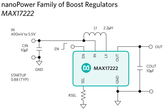 The Maxim MAX17222 not only offers the lowest quiescent current, but also minimizes heat dissipation and shutdown current. In True Shutdown™ mode, the minuscule 0.5 nA current draw virtually stops battery drain, providing longer runtime and eliminating the need for external kill switches. Dramatically reducing the size of the solution compared to other similar products, the MAX17222 is internally compensated and requires only a single configuration resistor and a small output filter for a complete power solution. For ease of use, the boost regulator comes in small standard 0.88 mm x 1.4 mm 6-Bump WLP and 2 mm x 2 mm 6-Pin μDFN packages with optimized density. It operates over a temperature range of -40 to +85 degrees Celsius.
Availability and Pricing
• The MAX17222ELT+ and MAX17222EVKIT# evaluation kit are available.
• The EE-Sim® model is available
. • Other products in the nanoPower family will be available in 4-6 weeks; products differ based on input/output current levels.
• Watch a nanoPower video, as well as an overview of the new boost regulators, comparators, op-amps, and supervisors: https://www.maximintegrated.com/nanopower