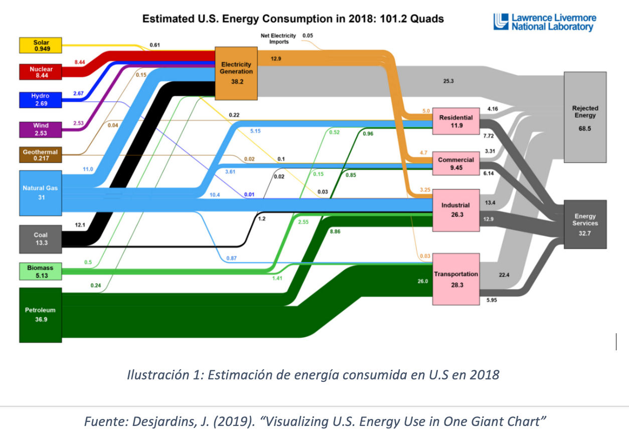
Therefore, one of the research areas of interest is the conversion of heat into electricity.
Thermoelectric modules have gained traction in recent years due to their great potential for generating electrical energy from temperature differences in devices and portable power supplies. Thermoelectrics are a type of device that converts thermal energy into electrical energy using the Seebeck effect.
These devices are based on the properties of certain materials that, when subjected to a range of temperatures, transform heat into an electrical voltage. Conversely, when a voltage is applied, they become hotter on one side and cooler on the other. Electrons move from the hot end of the material to the cold end, creating positive and negative electrodes and thus the electrical voltage. This effect, known as the Peltier-Seebeck effect, is completely reversible and is a property present only in a limited range of materials.
The main materials used in thermoelectric devices are P-type and N-type semiconductors. The most commonly used semiconductor materials in thermoelectric devices are bismuth telluride, antimony telluride, and silicon-germanium, either over-doped (N-type) or under-doped (P-type). The fundamental challenge in creating efficient thermoelectric materials is that they need to be very good at conducting electricity but not heat.
Most of these materials are metallic alloys. Certain metallic alloys, such as silicon-germanium compounds, can also be used to make thermoelectric devices. The highest yields currently available are epitaxial multilayer structures based on Sb₂Te₃/Bi₂Te₃, “Thin-film thermoelectric devices with high room-temperature figures of merit” (R. Venkatasubramanian et al., 2001), and quantum dot superlattices based on PbTeSe inclusions on a PbTe matrix, “Quantum Dot Superlattice Thermoelectric Materials and Devices” (TC Harman et al., 2002).
At the structural level, we find different types of thermoelectric devices, such as solid-state cells. These modules primarily require heat dissipation devices, such as radiators or extended surfaces. Another type of cell under development is the hybrid device (partially solid and partially printed). Currently, possible hybridizations are being studied in order to have a better optimization of the surface to which it has to be applied, both cylindrical and flat.
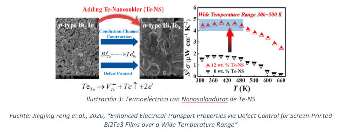
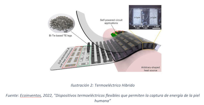 An example of this can be seen in the following article, “Enhanced Electrical Transport Properties via Defect Control for Screen-Printed Bi2Te3 Films over a Wide Temperature Range” (Jingjing Feng et al., 2020). This paper discusses screen-printed thin-film thermoelectric devices (TEDs), which are still in their early stages, primarily due to the low performance of screen-printed TEDs and, above all, their poor electrical transport properties.
A high-performance Bi2Te3 screen-printed sheet is designed and prepared by introducing Te-based over-welding (Te-NS) to simultaneously achieve conduction channel formation and defect control. On the one hand, the promoted carrier migration increases electrical conductivity sevenfold, with a power factor of 4.65 W*cm⁻¹*K⁻². On the other hand, the formation mechanism of the screen-printed Bi2Te3 sheet, following the introduction of Te-NS and bipolar conduction, is reduced by either increased bipolar generation of Bi2Te3 or greater suppression, resulting in temperature lag and maximizing the Seebeck coefficient.
Therefore, a high engineering power factor with excellent temperature linearity is achieved, indicating a potential application for screen printing. An open-circuit voltage of 11.34 mV and a maximum output power of 27.1 W are demonstrated at a temperature gradient of 105 K over a wide temperature range of 303 to 478 K. This study provides a theoretical and practical basis for improving the performance of screen-printed TE lamps and devices.
 However, most of the materials currently used are highly polluting; therefore, alternative solutions are being researched using less polluting materials that can be recycled and achieve efficiencies close to those of higher-performing materials (the Seebeck coefficient of bismuth telluride is 300 μV/K).
As alternatives to traditionally used materials, we can find lines of research and initial developments based on conductive polymers such as PEDOT:PSS, an intrinsically conductive polymer that has generated considerable interest since the discovery of its thermoelectric (TE) functions; carbon-based nanomaterials such as carbon nanotubes (CNTs) and single-walled carbon nanotubes (SWCNTs); metal alloys; and organic compounds.
In the case of the n-type single-walled carbon nanotubes (SWCNTs) discussed earlier, the following article, “Dual-Type Flexible-Film Thermoelectric Generators Using All-Carbon Nanotube Films” (Ryota Konagayay et al., 2023), discusses the increased performance of this material. The DFTEG achieved an output voltage of 40 mV and a maximum power of 891 nW for a temperature difference of 25 K between the cold and hot sides of the module. These are low performance results compared to those obtained with traditional materials such as Te, Bi, or Ge; however, it is a promising result for the development of thermoelectric modules using non-polluting materials.
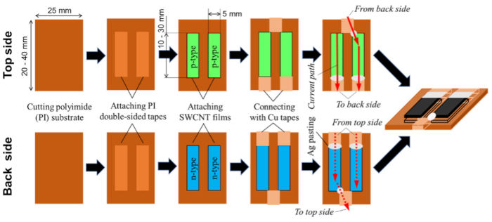 Figure 4: Schematic diagram of the DFTEG manufacturing process.
Source: Ryota Konagayay and Masayuki Takashiri, 2023, “Dual-Type Flexible-Film Thermoelectric Generators Using All-Carbon Nanotube Films”
Therefore, we can affirm that next-generation thermoelectric devices (made with more sustainable, flexible, and lightweight materials) have many potential applications for self-sufficiency. In electronics, these devices could be used to power wearable devices such as smartwatches and fitness trackers. In the field of sensors, these devices could be used to power temperature, pressure, and humidity sensors.
As thermoelectric device technology continues to advance, new materials and manufacturing methods are expected to be developed to improve the efficiency and scalability of these devices, potentially leading to solutions for greater energy efficiency and utilization.
AUTHOR: Vicente Milán, Engineering Researcher at AIMPLAS