


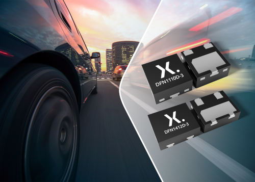
Nexperia's automotive-grade, discrete-lead-free packages range from the ultra-small DFN1006BD-2 (1 x 0.6 x 0.5 mm) to the DFN2020D-3 (2 x 2 x 0.65 mm), including the recently released DFN1110D-3 and DFN1412D-3. DFN devices can measure as little as 0.6 mm², offering PCB space savings of up to 90% compared to current SOT23 devices. Excellent thermal performance (Rth (j-sp)) allows for equal or better total temperature (Ptot) in the smaller DFN footprint. Simultaneously, these packages run cooler, improving overall system reliability. Nexperia's DFN package technology supports a Tj rating of up to 175°C.
Because automated optical inspection (AOI) is vital for some applications, especially in automotive, Nexperia pioneered the development of side-wetting edges (SWF) for DFN packages in 2010, and devices with SWF are now a proven and accepted solution. This allows for the inspection of solder joints visible after soldering. An additional benefit of DFN packages with SWF comes from the improved mechanical robustness of the bond to the PCB compared to devices without side-wetting edges. SWF enhances the board's shear strength and bending capabilities.
Mark Roeloffzen, Vice President and General Manager of Nexperia's Bipolar Discretes Business Group, comments: "With the DFN automotive package family, Nexperia offers engineers the choice: develop their application with current leaded SMD packages or with space-saving DFN technology. We are dedicated to leading the market with package innovation that meets customer needs and offers the broadest discrete portfolio in DFN technology.".
A large number of discrete semiconductors in DFN packages are already in volume production, and Nexperia will launch many more throughout 2020, resulting in the industry's broadest portfolio of such devices. Available types include high-performance standard products such as the BC847, BC817, and BAV99, and many more.