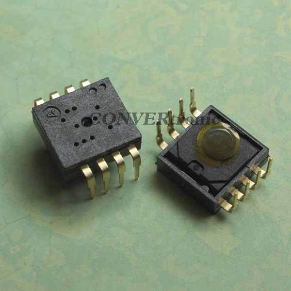



The new D-mode device features a conduction resistance of 20 mΩ and uses an 8 × 8 mm PQFN package with dual-side cooling (DSC). Renesas has begun sampling the component among OEM and ODM manufacturers of AI data center equipment.
The TP65H020G4PLSGBD is based on Renesas' GaN Gen IV Plus architecture and supports operation up to 700 V. Among its applications is the DC-DC intermediate bus converter (IBC) stage of 800 V architectures, responsible for reducing the voltage to levels of 48, 12 or 6 V.
The device is also aimed at battery backup unit (BBU) and capacitor bank (CBU) stages installed in auxiliary power racks of data centers.
One of the key features of the new component is its PQFN package with top and bottom cooling. According to data provided by Renesas, this configuration reduces thermal impedance on the top side by 10% compared to conventional packages cooled only on that side. The PQFN package measures 8 × 8 mm. Renesas indicates that its surface area is 57% smaller than that of its 10 × 15 mm TOLT package, allowing for a reduction in the space occupied by power devices on the PCB.
The company notes that the DSC encapsulation has been defined in collaboration with customers in the AI infrastructure sector with the aim of having a common format for this type of application.
The TP65H020G4PLSGBD incorporates Renesas' 650V GaN Gen IV Plus technology. Its features include low gate charging and output capacitance, as well as an integrated freewheeling diode with low reverse recovery. The device also features a threshold voltage that allows operation without negative gate bias.
According to Renesas, it can be controlled using a conventional gate driver for silicon devices, without needing to resort to a specific E-mode GaN controller.
The company also specifies switching capability in the MHz range, a feature that allows the use of smaller passive components in certain power conversion designs.
Renesas has used the new device in a 6 kW LLC DC transformer (DCX) reference design, responsible for converting 800 to 48 V. The system is controlled by a Renesas RA6T3 microcontroller and, according to tests provided by the company, achieves a power density of 2.6 kW/in³. In tests performed per module, the design recorded full-load efficiency 0.21 percentage points higher than that obtained with an equivalent board based on a TOLT package.
This last data corresponds to the complete reference design and the test conditions used by Renesas, so it should not be interpreted as a universal improvement in semiconductor efficiency compared to any TOLT solution.
The smaller package size also allows for modification of the FET layout on the board and reduces the PCB area used by the power stage. Renesas has also developed IBC DC-DC reference designs for 800V to 12V and 800V to 6V conversions using the 8 × 8 mm DSC platform.
The TP65H020G4PLSGBD can be combined with Renesas auxiliary controllers, gate drivers, and microcontrollers to develop the various power conversion stages of HVDC architectures. The company is targeting the new device primarily at OEMs and ODMs, as well as hyperscale operators developing 800V power infrastructures for AI data centers.
I have removed the corporate statement and expressions such as “industry's first,” “one of the lowest in its class,” “full strength,” “one-stop shop,” “extremely easy upgrade,” and general statements about cost reduction. The provided text does not offer a sufficiently broad market comparison to support some of these claims as independent facts.
I have also kept separate the 20 mΩ, 650 V and 8 × 8 mm package, which are device specifications, from the 6 kW, 2.6 kW/in³ and the 0.21 percentage point improvement, which correspond to the reference design and the tests described by Renesas.