Shocks, vibrations, and rapid thermal cycling to which these systems are subjected generate operational stresses inherent to missile systems, radar assemblies, avionics platforms, and space hardware.
The combination of higher performance requirements and demanding environmental conditions presents a challenge for system architects. The electrical, mechanical, and packaging decisions involved in the design of these platforms can no longer be addressed in isolation.
Stacked PCB architectures for high-density aerospace and defense systems
Printed circuit boards have long been the building blocks of electronic systems in aerospace and defense applications. They offer simple and repeatable manufacturing, combined with the ability to assemble components at high densities to efficiently utilize limited space. As systems become more compact and integrated, designers are increasingly relying on stacked PCB architectures to meet their stringent size, weight, and performance targets.

Figure 1. Internal structural components of a standard 1 unit (1U) CubeSat
Vertical stacking allows subsystems to be layered in confined spaces, typical of missile bodies and small satellite applications. It also allows for shorter signal paths between functional blocks. In high-speed digital and RF designs, reducing trace lengths directly improves insertion loss, timing margins, and impedance control.
The Z-axis, which represents the vertical connection between parallel plates or stacks, has therefore acquired strategic importance. A well-designed Z-axis interface allows for direct vertical stacking without sacrificing electrical performance or mechanical strength. However, achieving this balance in dynamic environments is not easy.
Challenges of traditional board-to-board connectors in harsh environments
As PCB density increases, traditional board-to-board connection designs are beginning to reveal their limitations. With the continued miniaturization of electronic components, connectors often become one of the largest elements on the PCB, competing with active circuits for limited space. The high pin count increases routing complexity, and mechanical loads from shock, vibration, and thermal expansion place additional stress on solder joints and connector pins.
Challenge Description
Large connector footprint Occupies a significant portion of the PCB surface in dense designs
Competition for board space Reduces the area available for active circuitry
Complexity due to the high number of pins Increases routing congestion and design difficulty
Mechanical stress transfer. Stresses soldered joints and pins during shock, vibration, and thermal expansion
Table: Challenges of traditional board-to-board connectors
In compact aerospace systems, access for inspection and repair is limited. A faulty soldered joint inside a stacked assembly can be difficult to detect and costly to repair. As assemblies shrink while environmental stresses remain constant, the margin for error narrows.
Historically, designers have relied on two main approaches to manage board-to-board connections in these high-performance applications.
Rigid mezzanine connectors
physically fix two PCBs in a fixed geometry. They offer easy vertical integration and predictable alignment. In controlled environments, this approach can be effective.
However, in systems subjected to strong impacts or thermal dynamics, the rigidity imposed by the soldered contacts becomes a disadvantage. When the boards experience differential expansion or mechanical acceleration, the stress is transferred to the connector pins and the soldered joints. Over time, this cyclic loading can lead to fatigue, cracking, and intermittent electrical failures.
The connector effectively becomes a structural element within the assembly. During missile launches or under the stresses imposed by recovery on aircraft carriers and rapid temperature cycles, fixed welded joints can compromise long-term reliability.
Jumper cables and flexible interconnects:
When rigid geometry cannot be guaranteed, or when dynamic environments must be considered, designers often use jumper cables or flexible assemblies. These provide mechanical decoupling between plates, reducing stress on welded joints and adapting to movement.

Figure 2: CIN::APSE Applications
However, cables add weight and consume valuable space. High-speed signal routing becomes more complex, as cables often emerge from the edges of PCBs. Strain relief must be carefully managed, and in high-acceleration (G) environments, a cable moving freely within a housing introduces its own reliability issues.
Signal integrity can also be compromised by longer interconnection paths, which increase insertion loss. The use of planar circuitry can further complicate impedance control at higher frequencies. Therefore, designers are forced to choose between the rigidity that transmits stress and the flexibility that introduces complexity.
Weldless compression connectors as a high-reliability solution for the Z-axis
Solderless compression interconnects offer an alternative to this traditional compromise. Instead of permanently attaching a connector to either board, compression systems establish electrical contact through a controlled mechanical load.
In a compression system, the contact elements are located between mating pads on opposing surfaces. Electrical continuity is achieved when a defined compressive force is applied along the stack. No soldered termination is required, and there are no rigid pins joining the plates. The interconnect is only activated when the assembly is mechanically mated.
How compression-based interconnects reduce stress and improve mechanical strength:
Compression connections enable direct vertical stacking that functions similarly to a mezzanine connector. Plates can be aligned in parallel and connected along a short, controlled path on the Z-axis. However, they achieve this without relying on soldered joints or free-moving cables. The contact elements are designed to conform to tolerances, absorb vibration, and respond elastically to differential thermal expansion. The interconnect is not rigidly fixed or floating freely within the housing but operates within a controlled mechanical enclosure. In dynamic environments where neither extreme is acceptable, compression solutions offer advantages in terms of stability, performance, and reliability.
Because the interface relies on controlled compression rather than permanent welded terminations, assemblies can be disassembled, inspected, and reassembled without thermal reworking. This facilitates on-site repairability and simplifies system maintenance throughout the product lifecycle.
CIN::APSE: a high-performance compression interconnect for the aerospace sector
CIN::APSE represents a mature development of solderless compression interconnect technology, specifically designed for high-reliability aerospace and defense applications. It is engineered to maintain stable electrical performance under shock, vibration, and thermal cycling, while supporting the dense, high-speed electronic architectures required by defense systems. The platform has achieved NASA Technology Readiness Level 9, reflecting its successful deployment in operational environments and demonstrating its maturity for mission-critical applications.
Key Features and Engineering Advantages of CIN::APSE Compression Interconnects
Essentially, CIN::APSE is a Z-axis interconnect system composed of precision insulators and compressible multi-wire contact elements arranged in configurable arrays. Each component plays a specific role in balancing alignment, flexibility, and electrical performance.
The insulator forms the structural backbone of the CIN::APSE assembly. Inside, each contact is housed in an hourglass-shaped cavity designed to:
· Contain the contact at its midpoint for precise alignment
· Provide flared ends that allow controlled self-alignment during compression
· Maintain dielectric isolation between adjacent contacts
· Define the allowable compression stroke for a constant Z-axis load
Each CIN::APSE contact consists of a compressible molybdenum wire bundle with a gold-plated exterior, offering:
· High conductivity and wear resistance
· Wide operating temperature range
· Multiple parallel conduction paths for redundancy
· Numerous micro-contact points for low and stable resistance
· Non-helical geometry to minimize inductive effects at high frequencies

Figure 3: Cross-section of the connector showing the compressible molybdenum wire bundle
When compressed between the coupling pads, the wire bundle establishes numerous micro-contact points, ensuring low contact resistance and stable electrical performance throughout the system's lifespan. This allows for the support of both high-speed digital signals and RF applications within the same architectural framework.
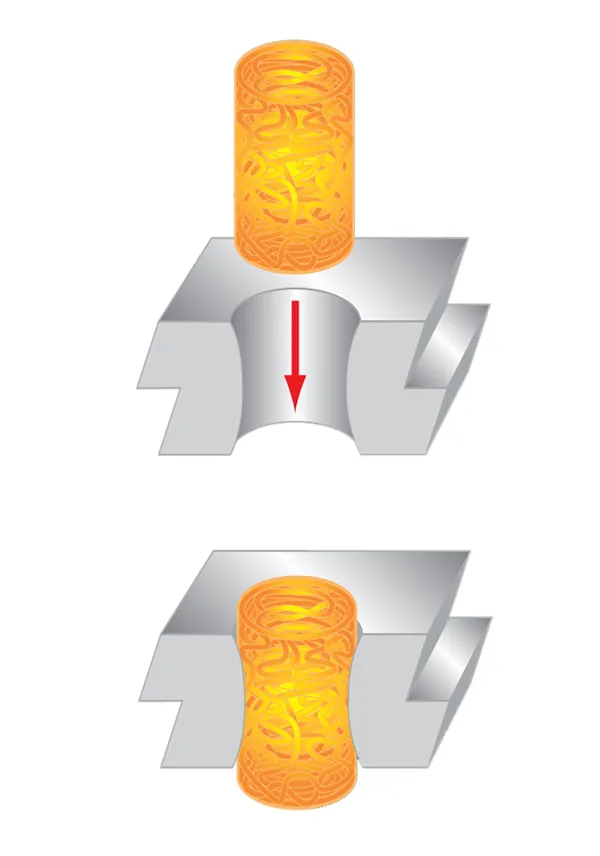
Figure 4. The basic CIN::APSE® contact configuration consists of a contact installed in a custom plastic insulator with the patented Cinch contact retention design. Once positioned, the contact extends to both sides of the insulator, creating an unparalleled electrical connection.

Figure 5. During installation, the CIN::APSE® interconnect is placed between two components—PCBs, flexible circuits, ceramic devices, etc.—with matching connection traces. The two components are then compressed and secured together.
One of the main advantages of CIN::APSE is its ability to be arranged in different geometric patterns, including:
· Square arrays — optimized for digital, power, and mixed-signal routing density
· Hexagonal arrays — offering uniform spacing and improved isolation for RF and microwave designs
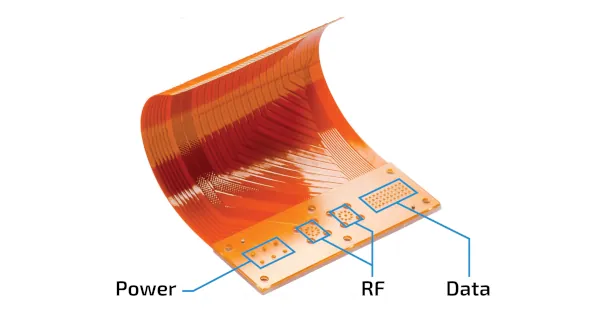
Figure 6. Flexible PCB with square and hexagonal matrices
The system can also be specified with custom heights and steps to support board-to-board, flexible-to-board, and LGA-type interfaces.
The future of compression-based Z-axis interconnects in high-reliability applications
As aerospace and defense electronics continue to evolve, connector designs must adapt to their needs. Higher data rates demand shorter, cleaner signal paths. Compact packages require efficient vertical integration. At the same time, assemblies must withstand shock, vibration, and thermal expansion without accumulating fatigue damage at their most vulnerable interfaces.
Rigid plate-to-plate connectors concentrate stress at the soldered terminations. Flexible cables offer mechanical freedom, but at the cost of density, control, and routing complexity. Compression-based Z-axis interconnects address the problem differently. By establishing electrical continuity through a controlled mechanical load rather than a metallurgical bond, they allow alignment and flexibility to coexist within a defined mechanical envelope.
In environments with stringent packaging constraints and tight reliability margins, the Z-axis interface becomes a critical element of the system architecture. Its mechanical behavior and electrical characteristics determine the long-term performance of the PCB stack and the underlying platform. For engineers evaluating next-generation stacking strategies, CIN::APSE offers a proven, compression-based approach aligned with the realities of high-reliability aerospace design.
Jerry Metcalf, Business Development Manager at Cinch