





In this article, we'll see how some of these peripherals work and how they can be combined to automate many of the low-level tasks that need to be managed in a typical microcontroller application.
Probably one of the most interesting but least understood peripherals within a typical RA microcontroller is the DOC – Data Operations Circuit. This can provide significant performance advantages in real-time applications by offloading simple tasks from the CPU, improving response time, and potentially reducing power consumption. This is especially true when the DOC is used in conjunction with other more advanced features available in the RA family.
At the heart of the DOC is a simple ALU – Arithmetic Logic Unit. This simple ALU has only three basic functions: it can perform a 16-bit data comparison, a 16-bit addition, or a 16-bit subtraction, and then generate an interrupt based on a specified condition. All these tasks can be executed without any CPU intervention by automatically transferring the data to be processed by the DOC, using a DMA controller or the Data Transfer Controller, which we will explain shortly. See Figure 1.
Figure 1: Simplified Block Diagram of the Data Operation Circuit (DOC).
When using the 16-bit comparison mode, an initial reference value is loaded into the DOC, then the 16-bit data to be compared is loaded and compared to the reference value in hardware. The DOC can be programmed to generate an interrupt in case of a true or false match.
When using 16-bit summation mode, an initial 16-bit value is loaded into the DOC. Then, additional 16-bit values (one or more) are loaded into the DOC and added to the original value. Once all the necessary values have been loaded, the system checks for overflow and, if necessary, generates an interrupt. This simple mechanism allows you to determine whether a specific threshold value has been exceeded, ideal, for example, for automatic level detection using the ADC.
When using 16-bit subtraction mode, an initial 16-bit value is loaded into the DOC. Then, additional 16-bit values (one or more) are loaded into the DOC and subtracted from the original value. Once all the necessary values have been loaded, an overflow check is performed, and an interrupt is generated if necessary. Again, this simple mechanism allows you to determine whether a specific threshold value has been exceeded.
However, the true power of the Data Operation Circuit lies in the fact that these three simple functions can be used to make straightforward decisions about how the system will operate, without any CPU intervention. This means we can make simple decisions directly in the microcontroller hardware, allowing the system hardware to decide how to handle the data it produces based on a simple comparison.
When combined with peripherals like the DMAC (Direct Memory Access Controller) or the DTC (Data Transfer Controller), which can be used to automate data transfer to the DOC, we can see how this can be used to create a system capable of making data-driven decisions from almost any source. This can be done without any CPU intervention, even when the CPU is idle. This can provide a much faster response to changing data, instead of waiting for the CPU to be interrupted before responding to the event.
We can imagine many cases where the DOC could be used; for example, when used with a UART interface, the DOC could be used to automatically detect an incoming address and alert the CPU when the address is valid. The DOC could be used with the analog-to-digital converter (ADC) in a level detection system to automatically detect when the level exceeds a programmed threshold. Using the DOC for these types of functions has many advantages. For example, the CPU could be dedicated to other high-priority tasks, and the DOC would only alert, via an interrupt, when a certain condition was reached. The CPU could be put into sleep mode to reduce power consumption and only wake up again via an interrupt on a valid alarm condition detected by the DOC comparison.
You can find the Data Operation Circuit (DOC) in all members of the RA family, and we have continued to improve the DOC's functions. The latest versions have additional features that allow even more complex data decisions to be made automatically.
Let's now look at the Data Transfer Controller (DTC) that we mentioned earlier. This is a peripheral designed to provide a simple yet extremely flexible mechanism for transferring data between a peripheral and memory, or between memory and a peripheral. A Data Transfer Controller can be found in all members of the RA microcontroller family.
The DTC uses a simple programmable controller to perform data transfers between memory and peripherals, and vice versa, while maintaining its configuration information in a table in SRAM. This is much smaller than using a large block of dedicated hardware for this task, such as the one typically used by the Direct Memory Access Controller (DMAC). This programmability provides a much greater level of flexibility compared to using a DMAC, and by storing the configuration table that describes the transfer in SRAM, we can have almost unlimited channels, limited only by the amount of available SRAM.
In the RA family, an event (or interrupt), triggered by the CPU, a peripheral on the device, or an external pin, can generate several actions on the device. You can see a simplified diagram of the interrupt controller in Figure 2. Here you can see that one event can trigger several actions: a traditional interrupt, which changes the application address; a DMAC transfer; or a DTC transfer. It is also possible to trigger more than one of these from a single event.
RA
interrupt controller
. The main advantage of this programmability is that it contains all the information necessary for the transfer in a small block of SRAM on the chip. This means that the DTC controller can be used not only to create one or two data transfer channels, but 10, 20, or even more if needed. The main disadvantage of this mechanism is that each transfer requires several cycles to read the configuration data stored in SRAM, so DTC transfers are typically slower than DMA transfers.
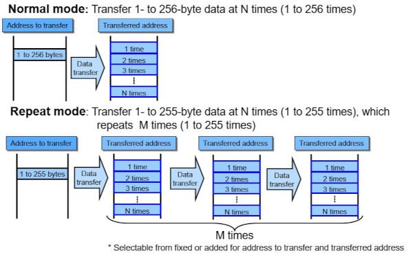
DTC can transfer one byte or more than one byte between a peripheral and memory, or between memory and a peripheral, up to 256 times. The source and destination addresses of the transfer can be the same or incremented or decremented independently, thus creating a buffer structure in memory.
At the end of the transfer, DTC can generate an interrupt to signal the CPU that the data is ready, or it can trigger a second DTC transfer. This can be used to chain multiple transfers, which is what we call, somewhat ironically, chaining mode. This chaining mode can be especially useful when multiple pieces of data need to be moved between peripherals and memory. Chaining mode is particularly interesting when used with the DOC discussed earlier, as it means that multiple transfers from various memory locations and/or peripherals can be triggered by a single interrupt source. For example, this means that with one interrupt, such as the ADC interrupt, we can load the comparison data into the DOC, and by chaining a second transfer, we can load the DOC with the ADC data for comparison—all completely automatically, without CPU intervention. This ability of an interrupt to generate a complex sequence of different transfers is extremely powerful, not only when used with the DOC. Figure 3 illustrates some of the different operating modes of the DTC.
Figure 3: Examples of Data Transfer Controller Operating Modes
The DTC can also be put into repeat mode, in which it will repeat the transfer an additional number of times. For most applications, the flexibility of the DTC offers a perfect balance between speed, flexibility, and, of course, device cost. Automated transfers between any peripheral and memory can be created with virtually no limit.
The Data Transfer Controller (DTC) provides an ideal method for automating data transfer between peripherals and memory without CPU intervention. Using the DTC in daisy-chain mode when transferring data to the DOC allows for simple testing of large amounts of data without CPU intervention, thus empowering the chip itself to make straightforward decisions.
Hopefully, you can see how the DTC can be much more flexible than traditional DMAC. If you require the highest data transfer speeds, DMAC remains the most appropriate method, and almost all RA microcontrollers include a number of DMAC channels. However, in terms of flexibility and data management, the DTC is far superior, allowing you to create multiple channels, limited only by the available SRAM.
Let's now see how the DTC and DOC can be combined with the ADC to create an intelligent analog sampling system that can operate entirely without CPU intervention, potentially reducing CPU demands and even saving power by turning off the CPU while the system is running. The system we want to create is a simple multi-input level detector that uses the 12-bit ADC's group sweep mode to sample each of the four input signals sequentially. Using the DTC and DOC combination, it detects whether a programmable threshold level is exceeded. Only if this value is exceeded will the system generate an interrupt and wake the CPU.
After the initial system setup, the CPU goes into sleep mode to conserve power and is only woken up by a DOC interrupt indicating that the threshold has been exceeded. Figure 4 shows a simplified schematic of the system.
 Figure 4: Simplified System Layout
I In group sweep mode, the ADC continuously samples each input in turn and copies the result to SRAM. Once all four inputs have been sampled, the ADC generates a DTC request. Using chain mode, this request initiates a chain of eight transfers between memory and the DOC, copying from the on-chip SRAM both the four ADC results and a corresponding threshold value against which each ADC result must be compared again.
ADC to DTC transfer request..
DTC transfer 1 Compare[0] to DOC. Chain Activated, the following transfer is performed
DTC transfer 2 AN000 to DOC Chain Activated, the following transfer is performed
DTC transfer 3 Compare[0] to DOC Chain Activated, the following transfer is performed
DTC transfer 4 AN001 to DOC Chain Activated, the following transfer is performed
DTC transfer 5 Compare[0] to DOC Chain Activated, the following transfer is performed
DTC transfer 6 AN003 to DOC Chain Activated, the following transfer is performed
DTC transfer 7 Compare[0] to DOC Chain Activated, the following transfer is performed
DTC transfer 8 AN005 to DOC Chain deactivated, stopped
In this case, we initialize the DOC to compare each value and generate an interrupt if any of the threshold values are exceeded.
Once the ADC, DOC, and DTC are initialized, each ADC input is continuously checked in the background, without CPU intervention. The CPU can handle other tasks or go into sleep mode and will not wake up until one of the inputs exceeds its corresponding value.
Many other low-level tasks can be automated by combining the DOC and DTC in a very similar way. This can be an extremely powerful technique for automating low-level functions and can save time and development costs in developing low-level software drivers for these tasks, as well as improve system performance by automating basic functions without requiring any CPU involvement.
Each member of the RA microcontroller family includes intelligent peripheral functions such as the Data Operator Circuit and the Data Transfer Controller, along with many other powerful peripheral functions that can also be used to create intelligent subsystems. Together, the DOC and DTC provide highly flexible and powerful solutions for automating low-level I/O functions in many different applications. Automating these low-level functions not only improves system response time to real-time events but can often reduce the complexity and size of the system software, thereby increasing reliability and reducing system testing costs.
The RA microcontroller family is intended for a wide range of communication and control applications, such as motor control, smart sensors, measurement, wearable instruments, low-power modems, and many other industrial and consumer applications, and is available in a wide range of memory size and package options. For more information, visit www.renesas.com/ra.
Author: Graeme Clark, Senior Product Marketing Specialist, Renesas Electronics





