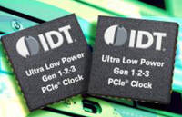
 IDT's new U-series of ultra-low-power PCIe buffers operates at the same supply voltage as modern SoCs and FPGAs, allowing designers to utilize the existing power line, thus reducing system complexity, physical size, and power consumption.
The 9DBU buffers are available in configurations from 2 to 9 outputs to meet virtually any PCIe application. They support fanless non-PLL and zero-delay PLL modes.
“IDT has led the timing industry in performance and power, and the latest family of devices further strengthens our leadership position,” said Dave Shepard, Vice President and General Manager of Timing and RF at IDT. “SoCs and FPGAs are trending toward lower supply voltages, and IDT is expanding its portfolio of PCIe timing solutions to address this trend. Our 1.5V solutions take advantage of the low-voltage power savings while simultaneously enabling customers to consolidate power lines to reduce system complexity. The new timing solutions complement IDT’s V-Series of 1.8V PCIe timers for the communications, computing, and consumer markets.”.
Device options include external and internal terminations, allowing designers to choose between maximum flexibility with external termination circuitry or maximum space savings with internal terminations. The entire family operates from a 1.5V supply, resulting in the lowest power consumption in the industry for PCIe timing devices. Eight-output devices use only 40 milliwatts, reducing cooling requirements and lowering operating costs.
The 1.5V U-series devices are pin-to-pin compatible with the widely adopted 1.8V IDT V-series, enabling easy replacement as SoC operating voltages continue to decrease. The 9DBU buffers are PCIe Gen 1, 2, and 3 compatible, so designers can use the same component across multiple product generations.
Samples of IDT 9DBU buffers are currently available to qualified customers. They are available in standard VFQFPN packages ranging from 4x4 mm to 6x6 mm.