
However, as the intrinsic performance of SiC chips approaches their theoretical limit, the focus of improvement shifts to another component of the module that has historically received less attention: the package.
The package is not merely a container. It is the structure that electrically connects the chips on the insulating substrate, forms the internal circuitry, and protects them from mechanical vibrations and environmental contaminants. And it is precisely this structure that is a significant source of parasitic inductance, additional losses, and lifespan limitations due to thermomechanical fatigue. To maximize SiC performance, more compact packages with lower power losses are required.
The solution: three-dimensional interconnection with PCB and conductive pins.
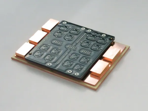
Fuji Electric has developed a three-dimensional (3D) wiring structure as a new packaging technology, aimed at achieving miniaturization and lower power losses in SiC power semiconductor modules.
The conceptual leap compared to conventional designs is substantial. Traditionally, wires and clips were used to connect the chips on the insulating substrate. In the new structure, this wiring has been replaced by a printed circuit board (PCB), which is connected in three dimensions by conductive pins pressed into the board.
The use of a PCB as an internal interconnection element is not trivial. Compared to the aluminum wires or copper clips that have dominated power packaging for decades, a PCB allows for defining current paths with much greater geometric precision, redistributing current more evenly among parallel chips, and reducing the effective length of current loops that generate parasitic inductance. The connection using pressed conductive pins —instead of soldered— adds an additional advantage in terms of reproducibility of the manufacturing process and control of thermomechanical deformation.
Quantified results: three simultaneous improvements
- Volume reduction: -50%
The new structure has reduced the product volume by approximately 50% compared to the conventional product. For an electric vehicle's propulsion system, where the inverter competes for space with the battery, motor, and cooling systems, a volume reduction of this magnitude in the semiconductor module has direct implications for the powertrain's mechanical design and the possibility of expanding the interior passenger compartment.
- Parasitic inductance reduction: -70% → switching losses -50%
Optimizing the current path using the 3D wiring structure has reduced the internal circuit's parasitic inductance by approximately 70% compared to the conventional product, resulting in a reduction of switching losses of approximately 50%.
This result warrants further consideration. Parasitic inductance in the switching loop of a power MOSFET module is directly responsible for the voltage overshoot that occurs during shutdown. The higher the loop inductance, the greater the voltage spike and the greater the required chip voltage margin—which penalizes both component selection and the maximum safely operable switching frequency. Reducing parasitic inductance by 70% means the chip can switch faster with less overvoltage, better utilizing the intrinsic capacity of SiC and reducing losses in each switching cycle.
- Junction life improvement: ×5
The conductive pin connection structure reduces the chip junction area compared to the conventional solution, and by relieving the stresses generated by thermal deformation at that junction, the junction life is improved approximately fivefold.
Solder joint fatigue is the primary degradation mechanism for power modules in traction applications, where thermal cycling is continuous and of high amplitude. The fact that the new conductive pin geometry — by reducing the contact area and better redistributing mechanical stresses — multiplies the life of the joint by five represents a qualitative leap in the reliability of the module, with a direct impact on maintenance intervals and the failure rate in the field.
Context: The Race to Electric Vehicle Range.
Electrified vehicles are expected to become widespread with the medium- to long-term shift towards decarbonization. Their powertrains consist of a motor and an inverter, which draws energy from the battery to power the motor. To overcome the challenges of improving range and increasing interior space, it is necessary to miniaturize the electrified powertrain and improve its efficiency.
The relationship between inverter losses and vehicle range is direct: every watt lost in the semiconductor module is energy that doesn't reach the wheel. At the typical power of a traction inverter (tens to hundreds of kilowatts), a 50% reduction in switching losses translates into a significant improvement in the overall efficiency of the system and, therefore, in the kilometers per charge.
Commercialization Roadmap
This technology will be applied to the company's power semiconductor modules throughout fiscal year 2026. Fuji Electric has a long track record in the development and manufacture of IGBT and SiC modules for traction, with a presence in both vehicle manufacturers and Tier 1 propulsion system suppliers.

Conclusion:
The 3D wiring structure developed by Fuji Electric represents a significant advance, not only because of the numerical values it achieves—half the volume, 70% reduction in parasitic inductance, half the switching losses, and five times the junction life—but also because of the coherence of the solution: a single design decision in the package simultaneously improves power density, efficiency, and reliability, the three parameters that determine the competitiveness of a SiC module in traction applications. With its planned implementation in 2026, the electric vehicle industry will have access to modules with a substantially better performance-to-volume ratio than the current generation.