Inter-Board Connectivity:
A mezzanine or daughter board can offer a practical solution for engineers to meet their design objectives. Stacking one board on top of another can help optimize space utilization within the case, simplify the main board design, allow for hardware customization for a specific market, or improve repairability.
Among the existing options for routing signals between two boards, a connector placed between them can streamline the connection and increase reliability, ensuring that the connections are mechanically robust and correct at all times. There are many options to choose from, ranging from low-profile connectors installed very close together when reducing overall height is a priority, to taller connectors to free up space for components on the main board or to facilitate airflow.
A single connector can simplify the design, and the two boards can be easily connected during product manufacturing. However, if the main board contains too many components or layers to allow all signals to be transmitted through a single connector, two or more connectors may be required. On the other hand, signal integrity problems could require the use of two separate digital signals from an analog signal or ensuring the optimal arrangement of the differential signals.
Exact placement
If more than one connector is needed, joining is more difficult since both parts of each connector must be properly aligned with the plates (Figure 1).
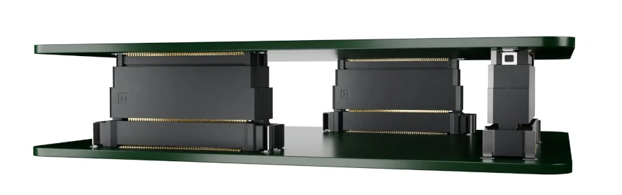
Figure 1. Positioning must be very accurate when joining two or more plates using connectors.
Connectors often have a small contact pitch on the order of submillimeters and, due to efficiency and accuracy, are assembled using the same automated processes as surface-mount components on circuit boards. While high-speed inline placement systems are extremely accurate, small errors can accumulate. The datasheet for a high-end machine might indicate a positional accuracy of ±0.035 mm. Similarly, screen printing machines can deposit solder paste with an accuracy of ±0.08 mm. Furthermore, tolerances for printed circuit board manufacturing can affect the positions of the solder points, and components may shift during soldering.
In the worst-case scenario, errors accumulating across the four halves of the joint between two separate connectors could be enough to stress the connector housings and solder joints when the connectors are joined. This stress can cause problems such as poor electrical contact and fracture of the connector body or soldered joint, and ultimately failure of the unit when subjected to end-of-line or field testing.
Adapting Connectors to Alignment Tolerance:
Among the existing options to avoid these consequences and ensure a precisely aligned joint free from potentially dangerous mechanical stress is the "floating" connector. These connectors, which allow movement of a series of contacts along the x and z axes, can accommodate misalignment and therefore reduce the dependence on absolute positional accuracy when joining plates containing multiple connectors.
For example, Harwin's Flecto range consists of fine-pitch connectors for connecting plates and provides a large number of pins—up to 160 connectors in a symmetrical double-row arrangement—and is based on a floating design that allows the male connectors to move up to ±0.8 mm from the connector's centerline on each axis.
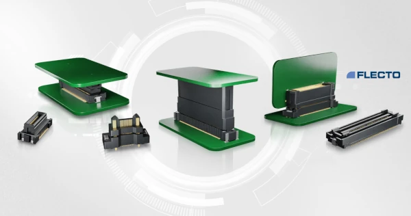
Figure 2: Floating connectors do not require absolute alignment.
Among the greatest challenges in developing floating connectors is ensuring proper mating after the initial connection, as well as maintaining consistent and continuous electrical contact between each connection. To achieve this, the contacts on the male side of the Flecto connector are designed to be flexible and are suspended from the housings. This ensures complete mechanical and electrical mating when the two parts are joined. The elasticity of the suspension mechanism ensures electrical integrity by absorbing shock and vibration to guarantee continuous contact.
While the connection sections are flexible to accommodate misalignment, pins at the base of the connector ensure overall positioning accuracy when inserted into the designated holes on the printed circuit board. Available connectors have interconnect pitches of 0.5 mm, 0.63 mm, and 0.8 mm, including a series with 0.5 mm pitch signal pins and 3.0 A power contacts. The power contacts are designed for easy blind soldering, and solderable posts through the board enhance positioning accuracy and mechanical strength. Signal-only connectors in this family utilize SMT anchoring elements to increase pull-out resistance.
High Data Transmission Speeds
: To help designers meet the demand for increasingly higher data transmission speeds in high-speed communication applications, the insertion loss, return loss, impedance, and near-end crosstalk (NEXT) of these connectors have been tested. Thanks to their NEXT of -40 dB or better across a wide frequency range, and their low insertion and return losses, Flecto covers applications such as machine vision, medical image processing, and electric vehicles. The performance of the F20 series, shown in Figure 3(a) and (b), allows these connectors to achieve data rates of up to 12 Gbit/s.
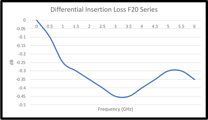

Figure 3 (a) and (b). Signal integrity test results.
Abstract:
Connecting stacked printed circuit boards often demands excellent accuracy if more than one connector is needed between the boards. Floating connectors not only allow for less absolute positional accuracy but also ensure signal reliability and integrity in numerous industrial, medical, and electric vehicle applications.
Developments in Connector Technology to Reduce Misalignment
Author: Ryan Smart, Vice President of Product, Harwin