Each technological advancement has enabled greater performance, increased efficiency, and miniaturization of power systems. But today we stand on the threshold of what could be the next quantum leap in power device performance toward the mythical 99.99% efficiency: the use of synthetic diamond as a semiconductor material, a truly exciting new concept for power electronics engineers.
Is the use of diamonds in semiconductors realistic?
The idea may seem exotic, not to say far-fetched, but, after all, diamonds are traditionally associated with jewelry, industrial applications such as abrasives and machinery for cutting, drilling, grinding and polishing, or in laboratories for high-pressure experiments, but not with power conversion systems or radio frequency amplifiers.
However, for many years, the scientific community has recognized diamonds as the ideal material for heat dissipation, as they exhibit thermal conductivity that far surpasses that of conventional materials like silicon. Nevertheless, the material's inherent hardness and the complexity of its processing had made it unsuitable for use in semiconductor technology.
Before delving into the subsequent debate on performance and advantages, it is essential to provide an overview of the evolution of diamond use in technological applications. The story begins in 1954, when General Electric (GE) successfully created the first synthetic diamond using the high-pressure, high-temperature (HPHT) method, marking the first instance of man-made diamonds. Following this milestone, the 1980s saw the initial expansion of diamond production using chemical vapor deposition (CVD), followed by the exploration of doping processes in the 1990s. Since then, researchers involved in the development of synthetic diamonds have expanded their knowledge of this material in terms of characterization, manufacturing, and processing.
However, advances in materials science and manufacturing techniques are rapidly transforming synthetic diamond into a contender for the future of semiconductors. Let's explore why diamond is considered a superlative material, how it compares to conventional and established WBG semiconductors (SiC and GaN), and what hurdles remain before it reaches commercial maturity.
The ladder of technical evolution.
We used to say that the evolution of power electronics is like a ladder with great leaps that bring new technologies from research to the market to improve performance, and diamond semiconductors could be considered the next step, although some consider it too great a challenge to be realized.
It's important to note that neither SiC nor GaN achieved immediate success. I recall that when SiC power diodes first entered the market in the late 1990s, they were expensive, difficult to manufacture, and suffered from reliability issues. GaN's commercial journey began later, finding its initial application in RF circuitry and subsequently evolving into high-efficiency power transistors for everything from fast chargers to data center power supplies.
There is no doubt that conventional silicon semiconductor technology is well-established and constantly improving with new technologies, although the success of SiC and GaN has been driven by an industry that required higher voltages, greater efficiency, and higher switching frequencies to reduce the size of end-use equipment. Today, SiC and GaN are present in everything from electric vehicles to solar inverters. WBG materials offered significant advantages in terms of size, weight, and power (SWaP), and we all enjoy powerful, efficient, and compact USB adapters.
GaN offered advantages in high-frequency switching due to its high electron mobility and low capacitance. Meanwhile, SiC found its niche in the medium- to high-voltage ranges, replacing silicon IGBTs and MOSFETs in applications such as electric vehicles and industrial drives. However, both SiC and GaN have their limitations, and some applications operating at high temperatures and in harsh environments may require higher levels of performance and robustness. This is where the properties of diamond not only appear superior but transformative.
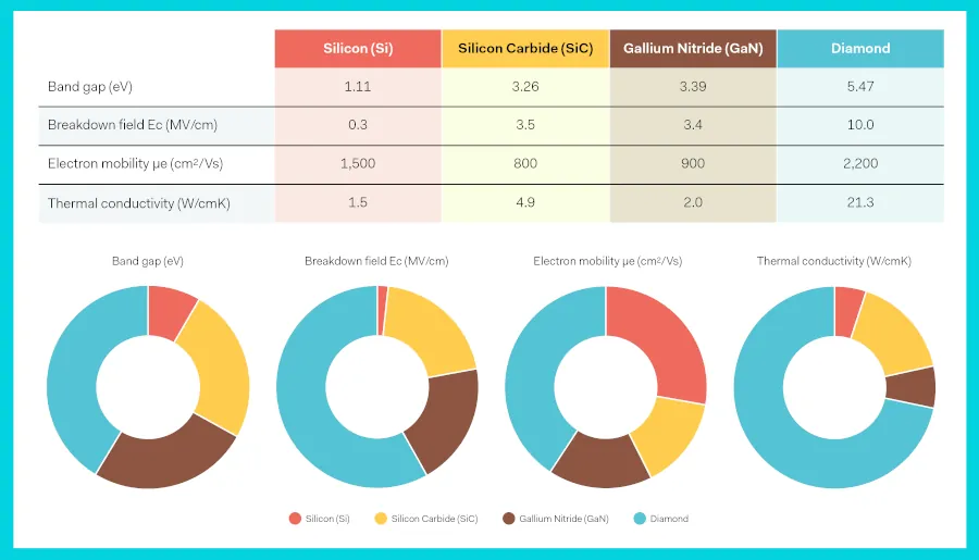
Figure 01: Material properties define performance (Source: PRBX)
Advantages of Diamond at a Glance.
To understand the potential of diamond, we must start with materials science. In semiconductor technology, the performance of materials for high-power, high-frequency, or high-temperature applications is determined by key physical properties. In the table (Figure 01), we present the fundamental properties of silicon, silicon carbide, gallium nitride, and diamond, and we have selected four key parameters that facilitate the comparison of the performance and advantages of the different materials:
Bandgap:
The bandgap, which indicates a material's ability to conduct electricity, is a fundamental criterion for determining its suitability for environments characterized by high temperatures or high energy levels. A wider bandgap indicates greater resistance to current leakage and breakdowns, which is crucial for applications in extreme conditions. In this respect, diamond far surpasses all other materials. Its wide bandgap of 5.5 eV allows devices to operate at higher voltages and temperatures.
Breakdown field:
The breakdown field is a measure of a material's resistance to electrical stress before conductivity occurs. It is crucial to understand that higher breakdown field values are essential for devices operating at high voltages, particularly in power electronics. This is because ensuring optimal performance under extreme electrical loads is paramount.
The theoretical critical electric field of diamond is nearly 10 MV/cm, three times greater than that of GaN or SiC and more than 30 times greater than that of silicon. This allows for the fabrication of thinner devices for the same voltage rating, reducing resistance and improving efficiency. It also opens the door to devices with power ratings of 10 kV, 20 kV, or even 50 kV, which could revolutionize high-voltage direct current (HVDC) transmission, electric railways, and grid-connected power systems.
Electron Mobility:
Electron mobility is defined as the speed at which electrons move within an electric field. It is a critical component of electronic switching and signal propagation, which occurs rapidly. Improving electron mobility in these devices leads to enhanced performance in digital circuits and high-frequency analog devices. Although GaN and diamond have similar electron mobilities, diamond devices can benefit from higher saturation speeds, enabling extremely fast switching with low on-state resistance and reduced losses. This could push switching frequencies to new heights, further miniaturizing magnetic components such as transformers and inductors.
Thermal Conductivity Assessment:
Thermal conductivity is a property of materials that quantifies their ability to transfer heat. In the field of electronics, high thermal conductivity is essential. This property is crucial for efficient heat dissipation, preventing overheating and improving the reliability and longevity of devices. Diamond's thermal conductivity, at 20 W/cmK, is the highest known of any material, making it exceptionally good for heat dissipation—a constant challenge in power electronics.
As we all know, thermal management is one of the most costly and limiting factors in high-performance systems. GaN, for example, often requires exotic substrates like silicon carbide to prevent overheating. Diamond's unparalleled ability to dissipate heat could allow devices to operate at temperatures exceeding 400°C without degradation, enabling more compact and robust systems, especially in aerospace and high-temperature applications.
Where do we stand today?
Despite the enthusiasm, diamond semiconductors are not yet in widespread production. However, significant progress has been made in the last decade, particularly in the fabrication of synthetic diamonds, spearheaded by chemical vapor deposition (CVD). CVD enables the production of large-area, ultra-pure single-crystal diamond wafers, a critical prerequisite for the reliability of semiconductor devices.
Currently, diamond power Schottky diodes and FETs with promising characteristics have been demonstrated in laboratories. However, large-scale commercialization is still in its early stages, limited by manufacturing costs, defect density, doping control, and scalability. Nevertheless, the latest research is very promising.
Some key developments:
In retrospect, I feel the same way I did when SiC and GaN were in the research phase. As a power electronics engineer, I immersed myself in numerous articles about broadband technology and its promises, wrote papers, and presented at conferences to share my enthusiasm with the power electronics community. Twenty years later, those promises have become a commercial reality.
After years of fundamental research, the use of diamond in the semiconductor industry is now moving into the next phase, which involves pre-industrialization and the development of an ecosystem to support future commercial products.
It is difficult, if not impossible, to list all the important steps that have been taken recently in the diamond semiconductor industry. As a French citizen working for a European company owned by the Japanese firm COSEL, I would like to share some notable projects in Japan and France (EU), but similar steps have undoubtedly been taken in the United States.
In Japan
, the first power circuit containing synthetic diamond semiconductors has been developed by a research team at a Japanese university. After exploring the hypothesis that diamond semiconductors have the potential to outperform silicon and other currently used materials, Professor Makoto Kasu of Saga University initiated research on diamond semiconductors and developed a functional diamond-fabricated n-channel MOSFET transistor.
Another crucial moment in the evolution of the Japanese semiconductor industry was the shutdown of the Fukushima Daiichi nuclear power plant, precipitated by the tsunami that followed the Great East Japan Earthquake on March 11, 2011. In the context of the reactor decommissioning process, a research initiative was launched in 2012 with the aim of developing diamond semiconductors that could function in the hostile environment of the damaged nuclear power plant, contaminated with high levels of radiation.
The initiative was made possible by the convergence of technical expertise from leading organizations such as AIST, the Japan Atomic Energy Agency (JAEA), Hokkaido University, and the High Energy Accelerator Research Organization (KEK).
The objective was clear: to design a critical monitoring system using diamond semiconductors capable of withstanding high levels of radiation, thus providing detailed data, including the neutron dose in the fuel debris. This initiative was undertaken to ensure safer and more efficient debris removal planning.
As part of this project, Ookuma Diamond Device Co., Ltd., a startup jointly founded by Hokkaido University and the National Institute of Advanced Industrial Science and Technology (AIST), established a vertically integrated system for the fabrication of diamond semiconductors, covering everything from substrate design to the assembly of the world's first differential amplifier circuit using diamond semiconductors, whose long-term operation in a high-temperature environment has been confirmed (300℃), resulting in the latest prototype shown in Figures 02 and 03.

Figure 02 - World's first amplifier circuit with diamond semiconductor operating at 300° C (572° F), patent pending (Photo courtesy of Ookuma Diamond Device Co., Ltd)
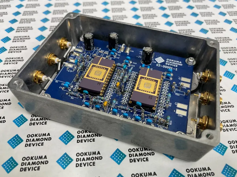
Figure 03 - Diamond MOSFET differential amplifier circuit (Photo courtesy of Ookuma Diamond Device Co., Ltd)
In early 2025, reports emerged of a significant breakthrough in the field of advanced semiconductor technology. The National Institute of Advanced Industrial Science and Technology (AIST), in collaboration with Honda R&D, successfully fabricated a prototype H-terminated diamond MOSFET. This breakthrough marked the first demonstration of high-speed switching operation at the ampere level, representing a major advancement in semiconductor research and development. The research team of Keita Takaesu et al. increased the substrate size and developed a parallel wiring technology to boost current (doi: 10.35848/1882-0786/adba3a). They plan to apply this technology to the next generation of mobile power devices. They are currently verifying and validating the preliminary results, which will pave the way for higher-current diamond MOSFETs.
In Europe:
Several projects were carried out in Europe, but it is worth mentioning the research and innovation framework program called Horizon 2020, which was launched in January 2014. The objectives of Horizon 2020 were to strengthen the EU's scientific and technological foundations, create a European Research Area with free movement of researchers and knowledge, and propel the EU towards a knowledge society and a competitive economy.
As part of Horizon 2020, a subproject called "Green Electronics with Diamond Power Devices," coordinated by the French National Centre for Scientific Research (CNRS), was created to explore the possibilities and feasibility of this promising technology. A consortium was formed for this purpose, bringing together experts in power device design, diamond growth and characterization, packaging and testing, as well as an innovative end user. Most of the partners also had experience with SiC or GaN technology, allowing the project to benefit from their extensive expertise and achievements in broadband semiconductors.
Among the most noteworthy reports published within the framework of this project, and as part of the next phase, I would like to mention the French company Diamfab, founded in March 2019 by CEO Gauthier Chicot and CTO Khaled Driche, and based at the Néel Institute-CNRS. Since its inception, Diamfab has established a collaborative network that contributes to the technological development of diamond synthesis and the development of cutting-edge components such as Schottky diodes and MOSFET transistors (Figure 04).
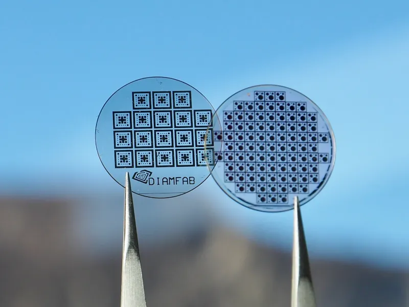
Figure 04 - Schottky diodes and power FET transistors on semiconductor diamond wafers, before packaging. (Photo courtesy of Diamfab)
In terms of research, the collaboration between the Néel Institute (CNRS), the Plasma and Energy Conversion Laboratory (LAPLACE, CNRS/Toulouse INP/University), and DIAMFAB is noteworthy. They have designed a diamond transistor that achieves a record-breaking volumetric current conduction of 50 mA. The component is a junction field-effect transistor (JFET) that utilizes volumetric conduction. The team successfully obtained homogeneous layers of boron-doped diamond, free of detrimental defects. This allowed them to increase the usable volume of the transistor and its gate, which reaches 14.7 mm² with 24 parallel fingers. The transistor is no longer just a miniature demonstrator but a truly usable component, which bodes well for the future of diamond transistor technology (Figure 5).

Figure 05 - (Left) Cross-sectional schematic of an elemental diamond JFET with the electrical measurement configuration. (Right) Optical microscope top view of an interdigitated diamond JFET at the end of the manufacturing process. (Photo courtesy of Diamfab)
Vision: Where can diamond take us?
Imagine inverters for electric vehicles with 99.9% efficiency, switching at 1 MHz and requiring no bulky cooling systems. Imagine ultra-compact space power modules that withstand extreme temperatures and radiation on the Moon or Mars. Or imagine smart grids operating at 100 kV with integrated sensors powered by diamond integrated circuits. These visions may seem futuristic, but so was SiC/GaN 25 years ago.
If development continues, diamond-based semiconductors could become the platform of choice for ultra-high-power, high-reliability applications within the next two decades. Governments and private sector players are increasingly investing in diamond R&D, viewing it as a strategic technology with implications for both energy and defense.
Conclusion: It's not just a flash, it's a beacon.
In the world of semiconductors, the material defines the limits, and diamond redefines those limits. Although it may still be years before it's ready for commercialization, the performance that diamond promises is too important to ignore. As power electronics continues to demand greater efficiency, higher voltage, and smaller form factors, the industry must keep a close eye on this gem of a material.
Just as we moved from silicon to broadband SiC and GaN to enable advances in electric mobility and renewable energy, the next frontier could well be forged in the hardest form of carbon, paving the way to the ultimate power semiconductor platform.
And just as we did with previous waves of innovation, those of us who work in this field must prepare ourselves, not only with technical knowledge, but also with imagination and curiosity.
References:
Powerbox (PRBX):
https://www.prbx.com/
SAGA University
https://www.saga-u.ac.jp/en/
Ookuma Diamond Device Co., Ltd.
https://ookuma-dd.com/en/
Honda R&D
https://global.honda/en/RandD/
National Institute of Advanced Industrial Science and Technology (AIST)
https://www.aist.go.jp/index_en.html
Ampere-class dual-pulse test of a half-inch H-terminated diamond MOSFET chip
Applied Physics Express 18, 036502 (2025)
https://doi.org/10.35848/1882-0786/adba3a
CNRS - Néel Institute
https://neel.cnrs.fr/en/institut-neel
Plasma and Energy Conversion Laboratory
https://www.laplace.univ-tlse.fr/en/home/
DIAMFAB
https://diamfab.com/
Currents exceeding 50 mA in interdigitated diamond field-effect transistors.
Damien Michez et al. – IEEE Electron Device Letters, 2024, 45 (11), pp. 2058–2061. ⟨10.1109/LED.2024.3453504⟩.
https://hal.science/hal-04687646v1/

About the author:
Patrick Le Fèvre, Marketing and Communications Director at Powerbox, is a seasoned marketing professional and a qualified engineer with 40 years of experience in the power electronics industry. He has been a pioneer in the commercialization of new technologies, such as digital energy, and in technical initiatives to reduce energy consumption. Le Fèvre has written and presented numerous articles and white papers at leading international power electronics conferences. These have been published over 450 times in media outlets worldwide. He also participates in various environmental forums, where he shares his expertise and knowledge on clean energy.
Patrick Le Fèvre
Director of Marketing and Communication at Powerbox