The presence of environmental interference can also negatively affect the signal. To address these issues, the 4-20 mA current-loop standard is commonly used for data transmission.
In current-loop systems, a transmitter is connected to a transducer that monitors a process variable, such as temperature, pressure, or flow rate. The transmitter is connected in series with a DC power supply and converts the transducer's output into a current ranging from 4 mA to 20 mA. 4-20 mA instruments and controls typically support alarm signals for conditions slightly below 4 mA and above 20 mA. For transmitters, current values below 4 mA and above 20 mA are used to indicate a fault. Recommendation NE43 was created to standardize how transmitters indicate faults and how control systems should interpret these signals, thereby facilitating better analog integration. The NE43 defines 3.8 mA to 20.5 mA as valid measurement values, indicating saturation from 3.8 mA to 4 mA and from 20 mA to 20.5 mA.
Thanks to the use of the 4-20 mA current loop standard, even if the voltage drops significantly due to long wires or if the loop voltage fluctuates because a large motor has been started elsewhere in the factory, it doesn't matter: the transmitter will maintain a constant current for a given process variable (see Figure 1). Another feature of this standard is that the device can also be powered from the current loop. In this case, the current consumption of the entire device must be a maximum of 3.5 mA.
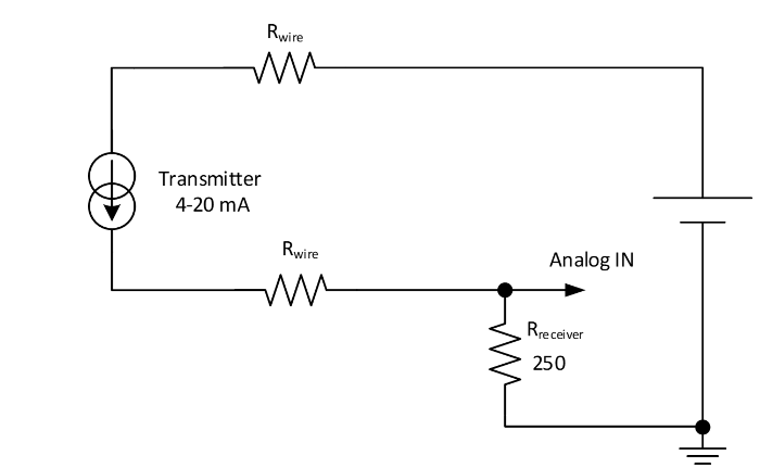
Figure 1. 4-20 mA Current Loop.
Among the various communication protocols in plant automation, the HART (Highway Addressable Remote Transducer) protocol stands out as the best overall solution for obtaining diagnostic and device information in digital format, while maintaining compatibility with legacy 4-20 mA automation architectures. Standard HART transmission uses frequency-shift keying (FSK) modulation. The standard FSK protocol frequencies are 1200 Hz (for binary 1) and 2200 Hz (for binary 0), and the communication rate is 1200 bits per second. An alternative to the standard FSK signal is a coherent signal with 8-way phase-shift keying (C8PSK). This project uses the standard FSK protocol.
Other versions of the protocol add support for pure sinusoidal or trapezoidal signaling. The former is more common, while the latter is primarily used when a very high data rate is required. In this project, the modem only operates with a sinusoidal signal. The resulting transmitted HART signal must be DC balanced and must not interfere with the analog signaling in any way.
The HART protocol follows the seven-layer Open Systems Interconnectivity (OSI) protocol model. The OSI model describes seven layers that computer systems use to communicate across a network. A HART modem operates at the physical layer (Layer 1).
Designed for industrial process measurement and control applications, HART is considered a hybrid protocol due to its combination of analog and digital communication. It can transmit a single variable using a 4–20 mA analog signal while simultaneously transmitting additional information in a digital signal. Figure 2 shows the basic schematic of a HART system.

Figure 2. Typical example of a HART system.
The digital information signal is transmitted using low-level modulation superimposed on the standard 4-20 mA current loop. Importantly, the digital signal does not affect the analog reading, as it is separated from the analog signal using standard filtering techniques.
Thanks to its integrated features and capabilities, the Renesas SLG47011 offers efficient performance in HART modem applications. Figure 3 shows the general schematic of the modem based on the SLG47011. With minor circuit modifications, it can function as both a host (control or monitoring system) and a field device (sensor). It should also be noted that, in addition to providing the basic functionality for the HART modem, the SLG47011 (like other GreenPAK integrated circuits) has many other logic blocks that can be used to implement additional customer-defined circuitry (such as a watchdog timer, etc.).
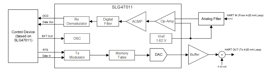
Figure 3. General schematic of the HART modem based on the SLG47011.
The modem receives signals with a duration of 833 μs through a 4-20 mA line and, after filtering them, converts them into bits using the UART protocol. Similarly, the modem sends signals, and the UART code converts them into a sine wave and sends them to the 4-20 mA line.

Figure 4 shows an example of the HART protocol signal.
Details of the external analog components of the HART modem

Figure 5. Schematic of the external analog section of the HART modem.
For proper operation and compliance with the official HART standard specification, the circuit includes an active filter that attenuates signals outside the 1200 to 2200 Hz range. This prevents noise in the current loop from affecting the correct demodulation of the packets. The operational amplifier U2 is configured as an active bandpass filter using the Sallen-Key topology, ensuring that only the relevant modulated signal is sent to the HART modem for further processing.
The circuit also features hysteresis to adjust the receive/reject threshold, controlled by resistors R3, R4, and R5. The hysteresis values are calculated to meet the HART specification requirements. Buffer U1 is connected to the output of the SLG47011 DAC, preventing it from being affected by the load. R1, R2, and C3 form the offset of operational amplifier U2. R6, R7, and C4 are used as a high-pass filter, while R8 and C5 form a low-pass filter.
This project uses an external 4 MHz clock to meet the specification requirements. However, thanks to the flexibility of the SLG47011, a different clock frequency can be used with minor design modifications. Furthermore, this example is designed for the modem to operate with a sinusoidal output with a peak-to-peak amplitude of 500 mV. Since this value is not standardized in the specification, the amplitude can be easily adjusted to suit the needs of any specific project.
Any low-cost amplifier with a bandwidth of at least 10 kHz and an output current greater than 1 mA can be used as an external operational amplifier. The input offset voltage value is not critical.
GreenPAK Design:
The SLG47011-based HART modem combines both current-loop signal modulation and demodulation. Figure 6 shows an internal layout of the modem in the Go Configure Software Hub.

Figure 6. Go to "Configure" > "HART Modem Schematic"
FSK)
to encode and transfer data, specifically a 1200 Hz signal for a binary "one" and a 2200 Hz signal for a binary "zero." First, the host transmits an active-low Request to Send (RTS) signal, activating the modulation mode. CNT7/DLY7 and CNT6/DLY6 are activated upon receiving this signal.
If a logic zero is transmitted to pin 4, the 4-bit LUT1 outputs a 222 kHz signal from CNT7/DLY7. If a logic one is present on the pin, it instead outputs a 121 kHz signal from CNT6/DLY6. The memory control counter counts from 0 to 100, corresponding to 101 samples of a sine waveform, providing the frequencies required by the HART protocol.
The ROM table stores the values for generating the sine wave, and the DAC converts this digital data from the ROM into a sine wave signal (without phase shift). This signal is then added to the current loop signal via a buffer.
To change the modulator's clock frequency, it is necessary to recalculate the number of samples into which the generated sine wave will be divided. Consequently, new values must be calculated in the memory table for the revised data. Additionally, new counter data values must be selected for CNT/DLY6 and CNT/DLY7 based on the new number of samples.
Figure 7 shows the waveforms for transmitting modulated data.
Channel 1 (yellow/top line) – HART OUT.
Channel 2 (light blue/2nd line) – PIN 4 (DATA IN).
Channel 3 (magenta/3rd line) – PIN 3 (RTS).

Figure 7. Sending data to the current loop (the data is 0x11)
Demodulator:
In this mode, the host's RTS signal is HIGH, which activates the demodulator's analog blocks (PGA and ACMP). The filtered current-loop signal is sent to the differential input of the programmable-gain amplifier (PGA), which amplifies the signal by 4Ω. Subsequently, the analog comparator (ACMP) compares this signal with the reference voltage provided by an external divider. Demodulation begins as soon as the SLG47011 detects a 1200/2200 Hz signal with a peak-to-peak VIN > 120 mV on the line (conversely, a sinusoidal signal with a peak-to-peak VIN < 80 mV will be ignored). These amplitude values are taken in accordance with the HART specification requirements, and the SLG47011-based solution meets this specification.
The CNT2/DLY2 delay removes noise from the comparator output, while P DLY acts as an edge detector. The CNT3/DLY3 delay and DFF21 determine which of two known frequencies is present at the input; specifically, a logic zero at the DFF output indicates an input frequency of 2200 Hz, and a logic one indicates 1200 Hz. The CNT4/DLY4 delay and DFF22 determine whether a sinusoidal signal is present at the input. A logic one at the DFF output indicates the presence of an input signal, while a logic zero indicates its absence. Simultaneously, the OCD (Output Carrier Detection) signal at pin 6 informs the host that the carrier has been detected. One Shot (CNT12/DLY12) generates an 820 µs output signal, which is sent via pin 8 to the host's data input.
Pin 13 (controlled by the 3-bit LUT4) and pin 16 provide hysteresis for the ACMPH in demodulation mode. In modulation mode, the reference divider is disconnected from the power supply to reduce power consumption.
Figure 8 shows the waveforms for data reception.
Channel 1 (yellow/top line) – HART IN.
Channel 2 (light blue/2nd line) – PIN 8 (DATA OUT).
Channel 3 (magenta/3rd line) – PIN 6 (OCD).

Figure 8. Current loop data reception
Conclusion
This article has analyzed how the SLG47011 integrated circuit can be used to implement a HART modem, handling both the modulation and demodulation of the HART signal. The design meets HART certification requirements but can be adjusted as needed to suit the specific requirements of each project. The main advantages of using the SLG47011 include low power consumption, flexibility, a compact size, and reliable performance, making it a practical choice for HART-compliant applications. For further information and testing, please refer to the lab demonstration video. The Renesas HART Modem Demo Board Manual is a useful resource for evaluating the modem's operation.
Author: Marian Hryntsiv, Senior Technical Documentation Applications Engineer, Renesas Electronics, Lviv, Ukraine