Growing Adoption:
SiC technology is on an upward adoption curve. Product availability has increased along with the breadth of options from multiple component suppliers. The market has doubled in the last three years and is projected to grow twentyfold to exceed $10 billion in the next 10 years. Adoption is extending beyond hybrid and electric vehicle (H/EV) applications to non-automotive motor and power control systems within trains, heavy-duty vehicles, industrial equipment, and EV charging infrastructure. Suppliers in the aerospace and defense sectors are also driving SiC quality and reliability to meet the stringent robustness requirements of components in these sectors.
A key part of a SiC development program is validating the reliability and toughness of SiC devices, as this varies considerably among suppliers. With the growing trend toward a whole-system approach, designers must also evaluate the scope of the supplier's product offering. It is important for designers to work with suppliers that offer flexible solutions, such as chip, discrete, and module options, backed by global distribution, support, and comprehensive design simulation and development tools. Developers looking to future-proof their designs will also need to explore the latest capabilities, such as programmable digital gate controllers, which address previous implementation challenges and allow for tuning system performance at the touch of a key.
Step One: Three Key Tests.
A trio of tests provides the data to evaluate the reliability of SiC devices: avalanche capability, short-circuit withstand capability, and the reliability of the SiC MOSFET body diode.
Adequate avalanche capability is critical: even a small malfunction of a passive component can cause transient voltage spikes that exceed the rated voltage limit, ultimately leading to device failure or possibly the failure of the entire system. SiC MOSFETs with adequate avalanche capability reduce the need for protective circuitry and extend the lifespan of applications. Top-rated options demonstrate high UIS capability of up to 25 joules per square centimeter (J/cm²). These devices show little parametric degradation even after 100,000 repetitive UIS test cycles.
The second key test is short-circuit withstand time (SCWT), or the maximum time before the device fails under a rail-to-rail short-circuit condition. The result should be similar to that of IGBTs used in power conversion applications, most of which have a SCWT of 5 to 10 microseconds (µs). Ensuring a sufficient SCWT allows systems to handle fault conditions without system damage.
A third key parameter is the forward voltage stability of the intrinsic diode of the SiC MOSFET. This can vary substantially from one vendor to another. Without proper device design, machining, and materials, the conductivity of this diode can degrade during operation, leading to an increase in the ON-state drain-source resistance (RDSon). Figure 1 sheds some light on the existing differences. In a study conducted by Ohio State University, MOSFETs from three vendors were evaluated. At one end of the results, all devices from vendor B showed degradation in forward current, while at the other, no degradation was observed in the MOSFETs from vendor C.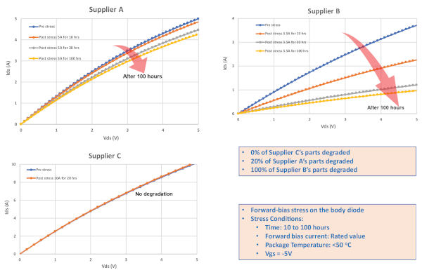 Figure 1: Forward characteristics of SiC MOSFETs, showing the differences in diode body degradation by vendor. Source: Dr. Anant Agarwal and Dr. Min Seok Kang, Ohio State University.
Once device reliability is validated, the next step is to evaluate the ecosystem surrounding these devices, including the breadth of product options, a robust supply chain, and design support.
Supply, Support, and System-Level Design:
Amid a growing number of SiC suppliers, today's SiC companies vary in device options, as well as in the expertise and infrastructure to support and supply many demanding SiC markets, such as automotive and aerospace/defense.
Power system designs undergo continuous improvement over time and within different generations of that design. SiC applications are no different. Early generations of designs may utilize widely available, standard, discrete power products within very standard surface-mount or through-hole package options. As the number of applications increases and designers focus on reducing size, weight, and cost, they typically move their designs to integrated power modules or may opt for a three-way partnership. These three-way partnerships include the final product design team, a module manufacturer, and a SiC die supplier. Each plays a critical role in achieving the overall design goals.
Supply chain issues are a key and legitimate concern in the rapidly growing SiC market. SiC substrate material is the most expensive component in the SiC die manufacturing process. Furthermore, SiC manufacturing requires high-temperature equipment that is not needed for developing silicon-based power products and integrated circuits (ICs). Designers must ensure that SiC suppliers have a robust supply chain model that includes multiple manufacturing locations in case of natural disasters or major performance issues to guarantee that supply can always meet demand. Additionally, many component suppliers are reaching the end of the lifecycle for previous generations of devices, forcing designers to spend time and resources redesigning existing applications instead of developing innovative new designs that would help reduce final product costs and increase revenue.
Design support is also critical, including simulation tools and reference designs that help shorten development cycle times. Thanks to solutions for controlling and driving SiC devices, developers can explore new capabilities, such as enhanced switching, to fully leverage the value of a total system approach. Figure 2 shows a SiC-based system design with an integrated programmable digital gate controller that further accelerates production time and creates new ways to optimize designs.
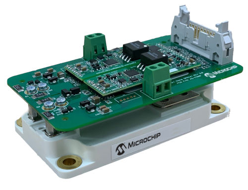 Figure 2: Module adapter boards combined with gate driver cores provide a platform for rapidly evaluating and optimizing new SiC power devices through increased switching.
New options for design optimization
Programmable digital gate driver options maximize the advantages of SiC through enhanced switching. They allow easy configuration of SiC MOSFET turn-on and turn-off times and voltage levels, enabling designers to accelerate switching and increase system efficiency while reducing the time and complexity associated with gate driver development. Instead of manually modifying the printed circuit board, developers can use configuration software to optimize their SiC-based designs with the touch of a button, future-proofing them while accelerating time to market and increasing efficiency and fault protection.
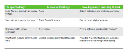 Figure 3: The use of programmable digital gate drivers to implement the latest augmented switching techniques helps solve SiC noise problems, speeds up response to short circuits, helps manage overvoltage problems, and minimizes overheating.
Early adopters of SiC are already reaping the benefits in the automotive, industrial, and aerospace and defense sectors, as its adoption expands into broader applications. Success will continue to hinge on the ability to validate the reliability and resilience of SiC devices. As developers adopt a total solution strategy, they will need access to comprehensive portfolios supported by a complete and reliable global supply chain and all the necessary design and development simulation tools. Furthermore, they will have new opportunities to future-proof their investments thanks to the new software-configurable design optimization capabilities that enable programmable digital door control.
By Orlando Esparza, Director of Strategic Marketing at Microchip