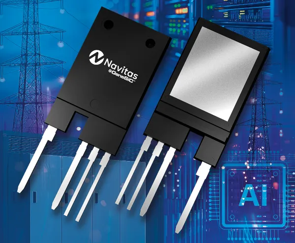
This package is specifically designed for GeneSiC SiC MOSFETs from 1200 V to 3300 V, offering module-like performance in a discrete and compact form factor. Compared to standard non-insulated through-hole packages, this package not only eliminates the need for external high-voltage insulation but also improves thermal performance and electromagnetic interference (EMI) suppression. This expands Navitas' package portfolio, which includes SiCPAK®, QDPAK, TO-247-LP power modules and other high-performance solutions, for more efficient, dense, and scalable power systems in the energy, grid, and AI data center sectors.
System advantages:
Integrated high voltage insulation: By integrating an aluminum nitride (AlN) substrate, this encapsulation offers solid high voltage insulation exceeding 6000 V, eliminating the need for external insulation materials and simplifying system design.
Direct cooling and reflow-compatible thermal management: A high-voltage, reflow-compatible insulated thermal pad allows the package to be mounted directly onto liquid- or air-cooled heatsinks, eliminating the need for an external thermal interface material (TIM). This reduces the RTH,J-HS by up to 60%, resulting in up to a 150% increase in power dissipation capacity, improving power density, reliability, ease of manufacturing, and overall system cost.
Reduced coupling capacitance and radiated EMI: The integrated high-voltage isolation reduces parasitic capacitance between the chip and the heatsink compared to external ceramic insulators, effectively minimizing common-mode noise and radiated EMI. This enables higher switching speeds and offers improved power density, increased system efficiency, and reduced system-level costs associated with EMI mitigation.
Superior power and thermal cycling life: Manufactured on a high-performance AlN substrate with active brazing (AMB) technology and a robust reflow-compatible heatsink interface, this package eliminates the need for external thermal interface materials (TIMs) and insulation materials in the system stack, providing superior power cycling capability and improved thermal cycling life.
Industry-standard form factor and footprint: Compatible with the established high-voltage TO-247-4 form factor and terminal geometry, this package enables easy system integration without redesign, while delivering superior performance, increased reliability, and a lower total system cost.
“High-power system design faces the fundamental challenge of balancing efficient thermal management with robust high-voltage insulation,” said Paul Wheeler, vice president and general manager of Navitas’ SiC business unit. “The UHV-TO-247-4-ISO package overcomes critical thermal management and insulation challenges, delivering power module-like performance in a discreet, compact form factor. As a high-efficiency building block, it enables system designers to fully leverage the potential of GeneSiC TAP SiC MOSFET technology in next-generation applications such as immersion-cooled and liquid-cooled power electronics.”
Product portfolio:
The UHV-TO-247-4-ISO package is offered in 3300 V, 2300 V, and 1200 V SiC MOSFET versions. This package advancement enables improved performance in grid-connected high-voltage power conversion systems (PCS), solid-state transformers (SSTs), battery energy storage systems (BESS), and renewable energy applications.