The residual ripple of these types of modules is often negligibly low, meaning that an output filter can be used in most applications. Since the input current to the buck converter emits pulses, this can generate radio frequency interference in the application. Depending on the specific application, the hardware developer decides whether to place an input filter directly before the power module or at another position on the switch. This article discusses the design process for input filters for optimized power modules and the measurement techniques used.
As a starting point, it is helpful to first illustrate how differential-mode noise is generated. Differential-mode noise consists of interference signals in a system with symmetrical reciprocal flow between the source and the load on the lines of a switching controller. It enters on one line and exits on the other.
 In the input circuit, the power supply module's clock frequency includes an AC component superimposed on the useful current and is similar in configuration to the current flowing through the power supply module's storage inductance. The input current flows into the input capacitor Cin. Real capacitors have a resistive component, the ESR, and an inductive component, the ESL, as shown in Figure 2.
Due to the ESR of the input capacitor and the impedances of the power supply module lines, the AC components produce an unwanted voltage drop.
 Thus, the noise voltage manifests as a differential-mode signal. The amplitude of the interference voltage at the capacitor's input depends primarily on the capacitor's ESR. Electrolytic capacitors have a relatively high ESR, ranging from just a few milliohms to several ohms. Consequently, the interference voltage can vary from a few millivolts to several volts. On the other hand, ceramic capacitors have a very low ESR of only a few milliohms, resulting in a noise voltage of a few millivolts. Furthermore, the design of the power supply module's circuit board exerts a strong influence on the interference voltage.
To reduce differential mode noise, at least one simple LC filter should be installed at the converter input to minimize AC line components. In high-impedance systems, such input filters can theoretically produce a voltage attenuation of 40 dB/decade in the attenuated band. In practice, a lower attenuation level is obtained because the terminal impedances have a reduced ohmic load and also because the components themselves exhibit losses. When sizing the LC filter, a cutoff frequency "f" - "c" is selected that is below the switching frequency "f" - "sw" of the power supply module. If the factor is one-tenth, theoretically, an insertion loss of 40 dB is achieved at the switching frequency where the highest spectral amplitude occurs. "f" -
"C" = " "f" - "SW" /"10" (1)
The cutoff frequency of an LC filter is generally:
"f" _"C" "=" "1" /("2π∙" √("L" _"f" " ∙ " "C" _"f" )) (2)
As an example for the calculation of the filter, an inductance of 10 µH is selected and equation (2) is transformed into:
"C" _"f" "=" "1" /(("2π ∙ 0.1 · " "f" _"sw" )^"2" "·" "L" _"f" ) (3)
Regarding the arrangement of the filter components, as shown in Figure 3, the filter capacitor can be placed on the voltage source side or on the input side of the power supply module. The decisive factor for attenuating the pulsed current from a voltage source is the inductance of the filter inductor.
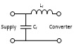 When the filter resonance is too high, oscillations can occur in response to changes in the input voltage that needs to be regulated. The stability criterion applied in this case is that the output impedance of the input filter "Z" _"out,filter" across a wide frequency range must be lower than the input impedance of the power module "Z" _"in,converter".
|"Z" _"out,filter" |"
Furthermore, the cutoff frequency "f" _"c" of the input filter must be well below the transition frequency "f" _"co" of the power supply module.
"f" _"c,filter" "≪ " "f" _"co,converter" (5)
Figure 4 shows how to do this, by placing an attenuator branch in parallel with the input of the power supply module.
 The attenuator reduces the quality factor of the input filter and, consequently, its output impedance at the resonant frequency. Equation (6) can be used to calculate the attenuation resistance "R" _"d" for a filter with quality "Q" _"f" "=1":
"R" _"d" " = √("L" _"f" /"C" _"f" ) (6)
A value that has become established in practice as an indicator of the attenuation capacitor's capacity "C" _"d" is a measurement of five to ten times the filter-capacitor capacitance.
"(5 ∙ " "C" _"f" ")
Alternatively, the filter can be attenuated by selecting an electrolytic capacitor that is switched in parallel with the filter output instead of the attenuator. As a general rule, the ESR value of the electrolytic capacitor is sufficient to attenuate the filter.
Selecting LC Filter Components:
Capacitors and inductors exhibit both capacitive and inductive properties in real-world applications. Filter inductors have their greatest filtering effect at their self-resonant frequency (SRF). In inductors, the SRF is strongly dependent on the inductance and the capacitive coupling between the winding turns. In capacitors, the SRF is strongly dependent on the capacitance and the length of their terminals. Therefore, when selecting filter components, it is recommended to ensure that the SRF is at the upper end of the frequency range where the RFI voltage is at its maximum, or, conversely, where the filter will be active.
The filter inductor is the decisive factor for differential-mode noise reduction, as it is the component that counteracts the rapid rise and fall of current in the input circuit. Figure 5 shows the impedance curves of three cylindrical-core inductors, based on an example from the Würth Electronics WE-SD product family.
 Higher inductance results in a lower SRF. It is recommended to select an inductor with an inductance value lower than the capacitance of the filter capacitor. In practice, a filter inductance with a maximum value of 10 µH is selected, as—depending on the design—such an inductance has a self-resonant frequency of approximately 30 MHz.
Exceeding the inductor filter current rating can damage the winding. Based on the switching controller efficiency, the effective input current of the power supply module can be calculated using equation (8).
"I"_"in" " = " ("V"_"out" " ∙ " "I"_"out" )/("V"_"in" " ∙ η" ) (8)
For safety reasons, a value higher than the filter coil's rated current should be selected.
The filter capacitor can be a liquid electrolytic capacitor, a polymer capacitor, or even a ceramic capacitor. The only consideration is that the filter quality at the cutoff frequency is sufficiently low (see section 4).
Other measures must be considered when sizing a Π filter. Ideally, the input filter should be placed as close as possible to the input of the power supply module. If the input filter is located at a greater distance, due to geometric constraints, the traces can act as an antenna between the input filter and the power supply module at higher frequencies. The trace inductance can also be used in conjunction with a ceramic capacitor to create an additional LC filter with a higher cutoff frequency (see Figure 6). Due to its negligibly low ESR, a ceramic capacitor can easily short high-frequency voltages to ground with low impedance.
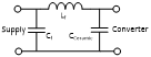 The capacitor's SRF should be approximately within the switching frequency spectrum of the power supply module. To illustrate this point, Figure 7 shows the impedance curves of WCAP-CSGP ceramic capacitors in size 0805 from Würth Elektronik.
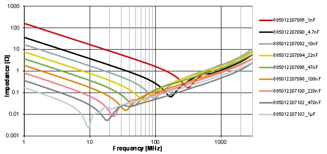 Of the components shown in Figure 7, at a clock frequency of 2 MHz, for example, a 1 µF capacitor would be suitable (resonant frequency marked in red). Even a 100 nF ceramic capacitor (resonant frequency marked in blue), which is used as a blocking capacitor in many electronic circuits, would be a suitable candidate at these values. It should be noted, however, that compared to the 1 µF version, the 100 nF capacitor has an ESR nine times higher.
Sizing an Output Filter:
Some power supply modules on the market, such as the MagI³C power supply modules from Würth Elektronik, exhibit negligible output ripple, making an output filter not strictly necessary. However, if the components supplied by the switching controller decouple interference signals via interfaces (e.g., sensor switches, analog switching circuits), an output filter may be required to filter the output voltage.
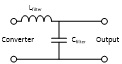 The circuit diagram shown in Figure 6 illustrates an output filter as a comparable option to the one shown here in Figure 8. It is generally not possible to make a definitive statement regarding the necessity and effectiveness of such an output filter, as it must be individually sized for each application. An output filter can be used to reduce the power supply module's ripple to an absolute minimum or, alternatively, to reduce undesirable subharmonic oscillations. The filter can be sized as already described in section 3. In this case, attenuation of the filter resonance is not necessary.
Noise Voltage Measurement:
Noise voltage is measured according to the basic standard IEC CISPR 16-2-1, which describes the types of interference variables that can be measured, the equipment to be used for different interfaces, and the measurement configuration for benchtop and floor-standing devices. Interference is evaluated in a frequency range from 9 kHz to 30 MHz. The measuring equipment includes, in addition to the EMI receiver, various line impedance stabilizers (LISNs), voltage detectors, clamp meters, and capacitive couplers. In a benchtop measurement configuration, as shown in Figure 9, the device under test (DUT) is placed on a non-conductive table on a reference ground plane. The table should be 40 cm high. If a vertical reference ground plane is also available, the table height should be at least 80 cm. The LISN must be connected to the ground plane to ensure good conductivity. The DUT itself and all connected cables must be positioned at least 40 cm from the ground plane.
 The cable length between the DUT and the LISN must not exceed 80 cm. The EMI receiver evaluates the asymmetric noise voltage that has been decoupled at the LISN for the different conductors of the cable.
Radiated Noise Measurement
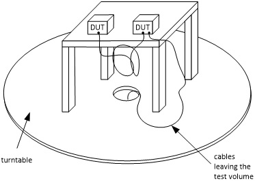
The method for measuring radiated noise above 30 MHz is described in the basic standard IEC CISPR16-2-3. The measurement environment is generally an anechoic chamber with a conductive floor or, on a smaller scale, an anechoic chamber. Here too, the DUT is placed on a non-conductive table (for portable or benchtop devices, see Figure 10) or on the floor. To allow the DUT to rotate on its own axis in its predetermined state during the measurement, it is placed on a turntable. In larger anechoic chambers, the receiving antenna is positioned 10 m from the DUT and its height is adjusted during the measurement to find the highest electric field strength at each of the measured frequencies (spectral peak). The antenna's orientation is also varied (horizontal and vertical polarization). In smaller anechoic chambers, the distance between the antenna and the DUT should be 3 m. Since the antenna height must be corrected, the height scan is omitted, and the ground between the antenna and the DUT must be covered with an absorbent material.
 Case study – Noise voltage measurement
The following section describes the measurement of noise voltage using a Würth Elektronik MagI³C power module evaluation board, equipped with an adjustable step-down regulator module (171 020 601) as an example.
Even during the preliminary phase, it is possible to measure the AC component at the power supply module input using an oscilloscope. By performing a time-domain analysis, the expected interference spectrum can be estimated at the start of the filter design process.
Figure 11 shows an 80 mV AC component, measured at a power supply module input voltage of 7.5 V, an average input current of 1.2 A, and an average load current of 2 A. Switching controllers can exhibit negative differential resistance from a power supply perspective. The input current increases as the input voltage decreases. For this reason, the noise voltage is measured under "worst-case" conditions: minimum input voltage, maximum current.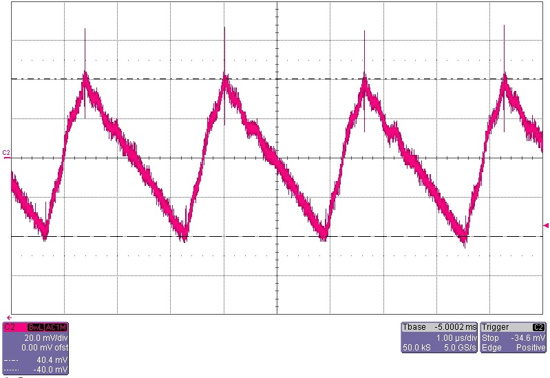 However, the decisive factor in analyzing this type of noise emission remains the noise voltage measurement, such as those performed in an EMC laboratory. Figure 12 shows the result of a noise voltage measurement without an input filter.
This power supply module operates at a clock frequency of 370 kHz. In the interference spectrum, the highest amplitude (red peak: 68 dBµV) can be measured at this frequency. The noise voltage amplitude density drops at a rate of approximately 40 dB/decade, meaning that no significant interference can be observed above the 15th harmonic. However, only above the 9th harmonic is the interference level more than 10 dB below the limit for the standard detector (dark blue line).
 Equation (3) from section 3 can now be used to calculate a suitable LC input filter. Due to the relatively low switching frequency, an inductor with a low SRF and an inductance of 4.7 µH is selected, and the filter capacitance is calculated.
"C" _"f" " = " "1" /(〖"(2π ∙ 0.1 ∙ 370 kHz)" 〗^"2" "∙ 4.7 µH" ) " = 3.9 µF" (9)
The selected filter capacitor will be the one with a capacitance slightly greater than 10 µF. The maximum input current is calculated using equation (8) from section 3.
This calculation requires the efficiency of the evaluation board, which is determined by measurement and in this case has a value of 91%.
"I" _"in " "= " "5 V ∙ 2 A" /"6 V ∙ 0.91" " = 1.83 A"
Based on the calculations of the filter inductance and input current, an appropriate inductor can now be selected. For this purpose, an unshielded inductor from the Würth Elektronik PD2 series, size 5820, has been selected. Figure 13 shows the result of a noise voltage measurement with the previously determined filter.
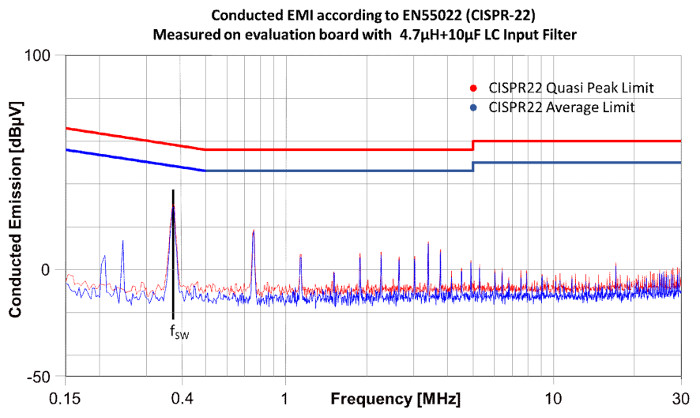 The interference level measured at the 370 kHz switching frequency is 30 dBµV. The levels of all harmonics are below 20 dBµV and are therefore sufficiently attenuated. The average level at 370 kHz corresponds to the maximum level and is 18 dB lower than the average limit of 47 dBµV. In practical measurements of conducted interference, a signal-to-noise ratio of this magnitude is perfectly sufficient to confirm the accuracy of this measurement.
The purpose of measuring the noise voltage is to demonstrate the usefulness of analyzing interference potentials in the time domain; however, a frequency domain analysis remains essential.
Finally, the equations in Section 3 can be used to calculate an attenuation resistor.
"R" _"d" " = " √("4.7 µH" /"10 µF" ) " = 0.686 Ω"
The higher the value of the attenuation resistor, the greater the attenuation of the filter resonance. In this case, the next largest resistor from the E12 series of 1 Ω can be selected.
A value of 47 µF is selected for the attenuation capacitor. This could be, for example, a Würth Elektronik eiCap ceramic capacitor from the WCAP CSGP series.
Measurement according to IEC CISPR 22.
The above measurements were performed according to IEC CISPR 16-2-1, as described in section 8. The use of a LISN enabled the asymmetric voltage decoupling and adaptation to the asymmetric voltage (common mode), which was subsequently compared with the limit obtained from the IEC CISPR standard for devices for private and commercial use (class B). For power supply components—and this includes all types of switching controllers—there is no directly applicable EMC standard. The entire application in which the switching controller is used must be assigned to a specific device category and then tested according to the corresponding standards applicable to the product or product family. In this case, the IEC CISPR 22 standard for IT installations was used only as a reference for the limits, which are also specified in the general standard IEC 61000-6-3. Generic standards can be used in cases where there is no specific standard for the device in question.
Abstract:
Regardless of the size of the AC component involved, an input filter remains an indispensable factor for successful EMC validation of a switching controller. Easy-to-apply equations can be used to calculate such an input filter individually. Considering the impedances of both the filter and the switching controller in the equations prevents oscillations and also ensures control stability for the switching controller itself. The specific selection of filter components lays the foundation for optimal filter design. With a suitable level of technical expertise in EMC testing methods, hardware developers can design their switches for specific purposes and, if necessary, make all kinds of adjustments to the filter itself.
Authors: Ranjith Bramanpalli and Steffen Schulze