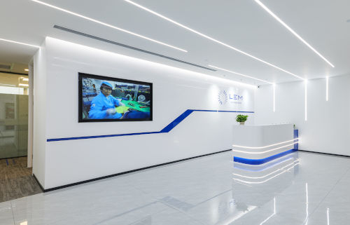
The center in China will feature state-of-the-art laboratory equipment, while the one in Germany will focus on ASIC (application-specific integrated circuit) design and semiconductor technology. This will help accelerate LEM's innovation in the integrated current sensor (ICS) segment.
This new investment in R&D centers in Europe and Asia follows LEM's recent opening of a cutting-edge factory in Malaysia incorporating advanced manufacturing technology. LEM's investment in the state of Penang was a recognition of the region's expertise in ASIC technology and its specialization in semiconductor design and production. The Penang factory is the latest example of LEM consolidating its operations and diversifying its global footprint to better serve its customers through a combination of advanced production facilities and skilled personnel.
LEM is now supporting this significant investment in production capacity and flexible supply with R&D capabilities designed to complement its existing center in Lyon, France, which opened in 2017, and to leverage existing R&D activities in Sofia, Bulgaria, now from its new city-center office. The development team at the new Munich semiconductor plant, led by Matthias Tänzer, will collaborate closely with LEM’s existing integrated current sensor (ICS) team in Geneva, Switzerland. There are currently 10 employees in Munich, and this number will increase in line with LEM’s ambitious expansion plans for the site.
On the other hand, the 1,400 m² center in Shanghai has 30 employees and the capacity to double or even exceed this number in the future, with a significant focus on research and development (R&D). This reflects LEM's commitment to innovation and growth in the sensor sector.
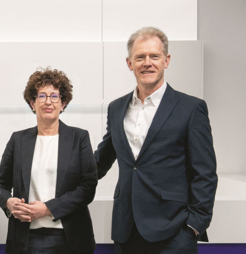 Verena Vescoli, CTO of LEM, emphasizes: “As leaders in electrical measurement, we firmly believe that integrated current sensing is a key part of our future growth and competitive advantage. It is vital that our integrated current sensor (ICS) offering meets our customers’ needs. The new R&D center in Munich will allow us to accelerate integrated circuit design and expand our ICS portfolio. It is always a pleasure to see different teams collaborating to share their expertise in ICS design and applications. I am very excited about the growth potential that the new centers in Munich and Shanghai will represent.”
John McLuskie, SVP of LEM in Asia, adds: “In an increasingly competitive market, we continue to invest in the future to develop solutions that are valued by our customers. China is a major source of technology and innovation, both for our customers and for LEM. The new R&D center in Shanghai will work alongside the existing one in Beijing, allowing us to be physically closer to our customers and deliver solutions even faster.”