The IDTechEx report "3D Electronics/Additive Electronics 2024-2034: Technologies, Players, and Markets" analyzes each of these approaches in detail.
The report weighs the pros and cons of each approach with numerous case studies showing how different manufacturing techniques and materials meet the requirements of application opportunities in the automotive, consumer goods, integrated circuit packaging, and medical device sectors.
Applying Electronics to 3D Surfaces:
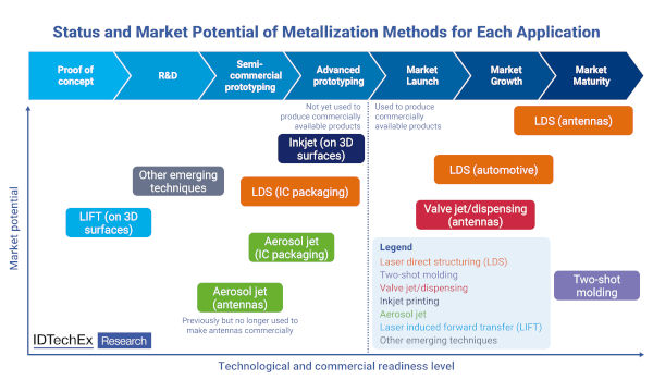
The most established method for adding electrical functionality to the surface of 3D objects is laser direct structuring (LDS). LDS experienced tremendous growth approximately a decade ago and is used to manufacture hundreds of millions of devices annually, including antennas and simple conductive interconnects on the surface of 3D injection-molded plastic objects. However, despite its high pattern-making speed and widespread adoption, LDS has some weaknesses that leave room for alternative approaches to surface metallization. For example, valve jet printing, also known as dispensing, is already used for a small proportion of antennas. This technique allows for the rapid deposition of a wide range of materials.
Aerosol jetting and laser-induced forward transfer (LIFT) are other digital deposition technologies covered in the report. These technologies offer higher resolution and faster deposition of a wide range of materials, respectively. Other emerging techniques include ultra-precision dosing, electrohydrodynamic printing, pulse printing, pad printing, and spray metallization. Gradual growth is expected in the partially additive electronics market, particularly in the telecommunications and microelectronics sectors.
In-mold electronics
(IME), in which electronic components are printed or mounted before thermoforming into a 3D component, facilitates the transition to greater electronic integration, especially when capacitive touch sensors and lighting are required. IME offers several advantages over conventional mechanical switches, such as up to 70% reduction in weight and material consumption, and much simpler assembly.
The IME manufacturing process can be considered an extension of the well-established in-mold decoration (IMD) process. This allows for the reuse of much of the existing process knowledge and equipment. IME differs from IMD by the initial screen printing of conductive thermoformable inks, followed by the deposition of electrically conductive adhesives and the assembly of SMDs (surface-mount devices, primarily LEDs today). More complex multilayer circuits can also be produced by printing dielectric inks to enable junctions.
Despite its advantageous characteristics, the commercial deployment of integrated SMD components in in-mold electronics (IME) has been quite limited to date. This relatively slow adoption, particularly in the core automotive interiors market, is attributed both to the difficulties in meeting automotive qualification requirements and to the range of less sophisticated alternatives, such as applying functional films to thermoformed parts. Along with greater acceptance of the technology, the adoption of IME will require clear design rules, materials that conform to established standards, and, above all, the development of electronic design tools. IDTechEx predicts that the most significant growth in 3D electronics will occur in in-mold electronics (IME) once it has passed its validation phase.
Fully Printed 3D Electronics:
Arguably the most innovative approach to additive electronics is fully printed 3D electronics, in which dielectric and conductive materials are deposited sequentially. Combined with placed SMD components, this results in a circuit, potentially with a complex multilayer structure, embedded within a 3D printed plastic object. The main value proposition is that each object and embedded circuit can be manufactured with a different design without the expense of creating masks and molds each time.
Fully 3D-printed electronics are therefore well-suited for applications requiring the short-term manufacturing of a wide range of components. The technology also holds promise for applications where customized form and even functionality are important. The ability of 3D-printed electronics to manufacture different components using the same equipment, along with the associated decoupling of unit cost and volume, could also enable a transition to on-demand manufacturing.
The challenge of fully 3D-printed electronics is that manufacturing is fundamentally a much slower process than injection molding, as each layer must be deposited sequentially. While the printing process can be accelerated by using multiple nozzles, it is best suited for applications where customization offers a tangible advantage. Ensuring reliability is also a challenge, given the varying properties of the materials; moreover, with embedded electronics, post-hoc repairs are impossible. One strategy is to use image analysis to check each layer and perform any necessary repairs before depositing the next.