

Challenges in Scaling Up Protrusions:
As welding steps decrease, several challenges arise. The reduction in protrusion height and joint surface area makes establishing reliable electrical connections increasingly difficult, requiring precise manufacturing processes to avoid errors. Critical coplanarity and surface roughness become paramount, as even minor irregularities can compromise the success of the joint.
Manufacturing faces challenges such as etching difficulties due to smaller copper columns and protrusion diameters, which increases the likelihood of undercutting. Electrochemical deposition (ECD) is more complex because ensuring uniformity and controlling coplanarity is more challenging. Furthermore, the sensitivity of bond quality to factors such as protrusion coplanarity, surface roughness, and hardness complicates the adjustment of parameters like temperature, time, and pressure as protrusion sizes decrease.
Conventional flip-chip bonding methods are limited to 50μm or 40μm steps, which raises reliability issues stemming from thermal expansion mismatches that cause die warping and displacement. To address these problems, the semiconductor industry is shifting to thermocompression bonding (TCB) for advanced fine-pitch bonding applications, including steps as small as 10μm. TCB offers a promising path to achieving the precision and reliability required in the ever-evolving semiconductor packaging landscape, pushing the boundaries of miniaturization and performance in electronic devices.
However, as the contact area decreases to around 10 microns, several problems arise. The smaller solder bead size increases the risk of intermetallic compound (IMC) formation, which reduces conductivity and mechanical properties. Furthermore, the possibility of solder beads touching and causing bridging failures during reflow processes can lead to chip failure. These limitations are becoming increasingly problematic in high-performance component packaging scenarios.
The emergence of hybrid Cu-Cu bonding:
To overcome these problems, hybrid Cu-Cu bonding technology is a game-changer. This innovative technique involves embedding metallic contacts between dielectric materials and using a heat treatment for solid-state diffusion of copper atoms, thus eliminating the bridging problem associated with soldering.
The advantages of hybrid bonding over flip-chip soldering are clear. First, it allows for ultra-thin pitch and small contact sizes, facilitating a high number of I/O points. This is crucial in modern semiconductor packages, where devices require an ever-increasing number of connections to meet performance demands. Second, unlike flip-chip soldering, which often relies on filler materials, Cu-Cu hybrid bonding eliminates the need for filler, reducing parasitic capacitance, resistance, and inductance, as well as thermal resistance. Finally, the reduced thickness of Cu-Cu hybrid bonding connections, which almost eliminates the 10–30 micron thickness of the solder balls used in flip-chip technology, opens up new possibilities for more compact and efficient semiconductor packages.
Challenges in the manufacture of the Cu-Cu hybrid junction:
The Cu-Cu hybrid junction technology is very promising for advanced semiconductor packaging, but it also presents a number of challenges that require innovative solutions for its future development.
Currently, there are three forms of hybrid Cu-Cu bonding (see the comparison table below). The wafer-to-wafer (W2W) process is the most widely used, while the die-to-wafer (D2W) or chip-to-wafer (C2W) process is the subject of intense research and development, as it can be used for many more applications that require the integration of dies of different sizes.
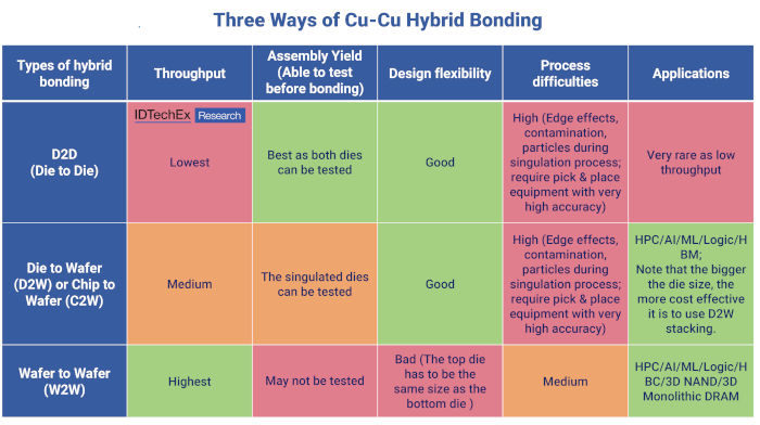
Three forms of hybrid Cu-Cu junction. Source: IDTechEx - "Materials and Processing for Advanced Semiconductor Packaging 2024-2034"
For all three methods, a crucial aspect of manufacturing is the bonding environment, where achieving a flat and clean dielectric surface through optimized chemical mechanical polishing (CMP) is essential. Furthermore, developing dielectric materials that can withstand lower annealing temperatures and shorter durations is crucial to minimizing the potential for wafer distortion and warping during the bonding process. Optimized electrochemical deposition (ECD) of copper solutions can also reduce annealing time and lower annealing temperatures, improving efficiency.
In the case of the D2W/C2W process, it will be crucial to address the challenges related to die uniqueness and edge effects, as well as minimizing contamination in dies and wafers. High-precision pick-and-place machines are needed to ensure accurate die placement, with tolerances as low as 0.2 µm. To account for potential placement errors, larger copper pads are essential. Furthermore, advanced thin-wafer handling technologies will play a significant role in ensuring the success of the hybrid copper-copper bond.
Future development of Cu-Cu hybrid junctions will likely focus on refining and optimizing these critical aspects of the process. This includes advancements in CMP, dielectric materials, ECD solutions, and pick-and-place machinery, as well as innovations in thin wafer handling. Overcoming these challenges will pave the way for wider adoption of Cu-Cu hybrid junctions in advanced semiconductor packaging, enabling the creation of smaller, more powerful, and more energy-efficient electronic devices.
To learn more about 3D semiconductor packaging (Cu-Cu hybrid junction), see the IDTechEx report "Materials and Processing for Advanced Semiconductor Packaging 2024-2034." The report is divided into four main parts, offering a structured approach to understanding advanced semiconductor packaging. Part 1 provides a comprehensive introduction to the technologies, development trends, key applications, and ecosystem of advanced semiconductor packaging, giving readers a solid overview of the field. Part 2 focuses on 2.5D packaging processes, delving into crucial aspects such as dielectric materials for RDL and Microvia, RDL fabrication techniques, and material selection for EMC and MUF. Each subsection in this part presents a detailed analysis of process flows, technology benchmarks, stakeholder assessments, and future trends, providing readers with a complete picture.
The report goes beyond the analysis of 2.5D packaging to reach its third part, which focuses on the innovative Cu-Cu hybrid junction technology for 3D semiconductor packaging (Cu-Cu hybrid junction). This section offers valuable data on the manufacturing process and guidance on material selection for optimal results. It also presents case studies highlighting the successful application of Cu-Cu hybrid junctions using organic and inorganic dielectrics. Furthermore, the report includes a 10-year market forecast for the advanced organic dielectric semiconductor packaging module, presented in the final chapter. This forecast covers both unit and area metrics, providing the industry with significant insights into projected market growth and trends for the next decade.
AUTHOR: Dr. Yu-Han Chang, Senior Technology Analyst at IDTechEx