

Compared to conventional electrical interconnections, photonic technologies can provide high bandwidth and reduce losses and energy consumption associated with transmitting large volumes of data. Furthermore, certain photonic devices can be integrated with CMOS processes and combined with electronic circuits.
These features are driving the use of photonic circuit-based transceivers for connections between servers, accelerators, and other nodes in data centers. According to IDTechEx forecasts, the market for these applications could reach $48 billion by 2036.
The role of indium phosphide in silicon photonics
One of the materials that plays a key role in these systems is indium phosphide (InP), a III-V compound semiconductor used, among other applications, to manufacture laser sources. Silicon has limitations for efficient light generation, so silicon photonics circuits are often combined with III-V materials to incorporate the necessary optical sources.
Optical transceivers have different architectures. One of them uses monolithic InP photonic circuits, in which elements such as lasers, modulators, photodiodes, and waveguides can be fabricated on the same material platform.
This approach reduces the need to subsequently attach an InP laser source to a silicon photonic circuit, although it requires a higher consumption of indium phosphide and uses manufacturing processes with smaller wafers and different yields than those of the silicon industry.
InP and silicon photonics are complementary technologies
Another architecture uses silicon for much of the photonic circuitry and reserves III-V semiconductors for functions that require their optical properties, especially laser sources. For this reason, the growth of silicon photonics does not necessarily imply a corresponding reduction in the demand for InP. It may, however, modify the type and quantity of indium phosphide components required for each system.
In a monolithic InP architecture, a significant portion of the circuit is fabricated from this material. In silicon photonics systems, consumption can be concentrated in specific devices, such as continuous-wave lasers that provide the optical source for silicon-fabricated modulators.
The Indian supply chain
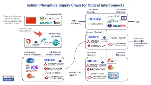
The increased demand for photonic components is putting the indium phosphide supply chain under scrutiny. Indium is primarily obtained as a byproduct of zinc production. According to data compiled by IDTechEx, approximately 70% of the global supply is concentrated in China.
This geographic concentration is a significant factor in the supply chain. In April 2025, China introduced export controls on several materials, including indium. These measures established licensing requirements for certain exports.
Once obtained and processed, indium is combined with phosphorus to manufacture InP substrates. The production of these wafers requires specialized processes and relies on suppliers such as Sumitomo Electric, AXT, JX Nippon, and Freiberger.
From InP wafers to photonic devices
After substrate fabrication, the wafers undergo epitaxial growth processes to deposit the different crystalline layers necessary to manufacture the devices. Among the techniques used are metal-organic chemical vapor deposition (MOCVD) and molecular beam epitaxy (MBE).
Components such as lasers and modulators are then fabricated on the wafers. These devices can be sold individually, integrated into InP-based optical transceivers, or combined with silicon photonics circuits.
A key difference compared to conventional silicon semiconductor manufacturing lies in the wafer size. While the silicon industry routinely uses 300 mm (12-inch) wafers, 2, 3, and 4-inch formats remain common in InP. In response to increasing demand, various manufacturers are working on larger diameter wafers. IDTechEx has identified projects aimed at advancing towards 6-inch InP wafers.
A production chain with high vertical integration
The indium phosphide industry also exhibits a high degree of vertical integration. Companies like Coherent and Lumentum control different stages of the chain, from wafers and epitaxial growth to the manufacture of devices, laser modules, and optical transceivers.
This model differs partially from that used in silicon photonics, where circuits can be manufactured in external foundries such as TSMC, Tower Semiconductor or GlobalFoundries and subsequently sent to companies specializing in assembly and testing.
The structure of the InP industry is linked to its historical use in specialized telecommunications applications, characterized by relatively small volumes and high-value products. The specific knowledge required for processes such as epitaxial growth has also led to different manufacturing stages remaining integrated within the suppliers themselves.
Demand for AI increases pressure on supply
The growth of infrastructure dedicated to artificial intelligence is changing this landscape. Data centers require higher-capacity optical connections to link servers, accelerators, and other processing systems.
This increase is raising the demand for photonic components and, with it, the need for InP-based devices.
According to IDTechEx's analysis, supply constraints are also favoring the development of silicon photonics architectures that use a smaller amount of InP, for example through external continuous-wave lasers combined with silicon modulators.
New materials for photonic circuits
Silicon and indium phosphide are not the only platforms being developed for future photonic integrated circuits.
Among the emerging materials is thin-film lithium niobate (TFLN), which is being studied for modulators and other high-speed photonic devices.
Another platform under development uses barium titanate (BTO), a material whose electro-optical properties may be of interest for certain switching and modulation applications.
These technologies are being researched for future generations of photonic circuits intended for communications, data processing, and quantum technologies.
The evolution of these platforms, along with the growth of silicon photonics and the availability of indium phosphide, will determine part of the development of the optical interconnects needed for data centers and high-performance computing systems.