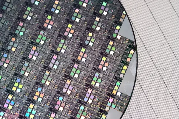
According to engineering data presented by both companies, the solution achieves accelerations of between 10 and 17 times in certain workloads, with the aim of facilitating the manufacture of advanced chips intended for artificial intelligence applications.
The complexity of advanced lithography increases computational demands.
The evolution toward more advanced semiconductor manufacturing nodes is increasing the complexity of lithographic patterns. Traditional optical proximity correction (OPC) and computational lithography techniques require ever-increasing processing power, especially with the transition to high-NA numerical aperture extreme ultraviolet (High-NA EUV) lithography. Adding to these demands is the use of advanced curvilinear patterns through technologies such as inverse lithography (ILT).
According to Siemens, the long computational times can limit the application of these techniques at the full-chip scale and force engineering teams to balance the depth of optimization with development timelines.
These limitations can hinder the identification of critical lithography points and impact process margins and manufacturing performance of advanced AI processing and memory devices.
NVIDIA cuLitho Integration in Siemens Calibre:
This collaboration combines the capabilities of Calibre software with GPU acceleration provided by NVIDIA cuLitho. This integration enables faster lithographic simulations and more comprehensive optimization processes before chip design completion (tapeout).
Siemens and NVIDIA note that the resulting acceleration facilitates the application of advanced pattern generation strategies, including curvilinear inverse lithography, at manufacturing scale.
Ankur Gupta, Executive Vice President of Siemens' EDA IC portfolio, emphasizes that combining Calibre with NVIDIA's GPU acceleration allows for the application of advanced computational lithography techniques that traditionally required significant computing resources. Tim Costa, Vice President and General Manager of Industrial and Computational Engineering at NVIDIA, points out that this integration enables the handling of increasingly complex patterns and expands the optimization capabilities needed to manufacture advanced semiconductors.
10-17x Speed Reduction in Lithographic Simulations:
Engineering results reported by Siemens and NVIDIA show speed improvements of 10-17x in certain computational lithography workloads. The reduced simulation times allow semiconductor and photomask manufacturers to perform more optimization iterations in less time. It also facilitates the early detection of critical lithography points and the improvement of manufacturing process margins before tapeout.
According to the companies, these capabilities contribute to making the use of full-chip curvilinear patterns viable in High-NA EUV-based manufacturing processes.
Applications in AI Semiconductor Manufacturing:
The integration of cuLitho into Calibre is geared towards chip and photomask manufacturers working with advanced lithographic processes. The accelerated simulations allow for expanded optimization tasks without a proportional increase in computation time, a crucial factor for the processing and memory devices used in AI infrastructures. Siemens and NVIDIA believe that reduced execution times can accelerate the preparation of manufacturing processes and facilitate the introduction of new generations of AI semiconductors.
With these advancements, both companies are expanding their collaboration in GPU-accelerated computational lithography, combining the Calibre manufacturing tools with NVIDIA cuLitho to address the demands of advanced lithographic patterns.