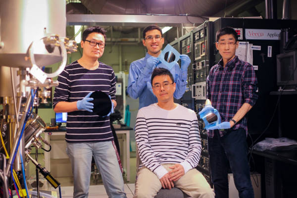
A new technique developed by MIT engineers can reduce the overall cost of wafer technology and enable devices made with more exotic, higher-performing semiconductor materials than conventional silicon.
The new method uses graphene, single-atom sheets of graphite, as a kind of "copying machine" to transfer intricate crystalline patterns from an underlying semiconductor wafer to a top layer of identical material.
The engineers developed carefully controlled procedures for placing individual sheets of graphene onto an expensive wafer. They then created semiconductor material on top of the graphene layer. They found that graphene is thin enough to appear electrically invisible, allowing the top layer to see through the graphene to the underlying crystalline wafer, imprinting its patterns without being influenced by the graphene.
Graphene is also quite "slippery" and doesn't tend to stick to other materials easily, allowing engineers to simply peel off the top semiconductor layer of the wafer after its structures have been imprinted.
Jeehwan Kim, a professor in the departments of Mechanical Engineering and Materials Science and Engineering, says that in conventional semiconductor manufacturing, the wafer, once its crystal pattern is transferred, is so tightly bonded to the semiconductor that it is almost impossible to separate without damaging both layers.
“You end up having to sacrifice the wafer; it becomes part of the device,” Kim says.
With the group’s new technique, Kim says manufacturers can now use graphene as an inner layer, allowing them to copy and paste the wafer, peel off a copied film from the wafer, and reuse the wafer many times. In addition to saving on wafer costs, Kim says this opens up opportunities to explore more exotic semiconductor materials.
“The industry has been stuck on silicon, and although we’ve known about better-performing semiconductors, we haven’t been able to use them because of their cost,” Kim says. “This gives the industry freedom to choose semiconductor materials based on performance rather than cost.”
Kim's research team discovered this new technique at the MIT Electronics Research Laboratory. Kim's MIT co-authors include first author and graduate student Yunjo Kim; Samuel Cruz, Babatunde Alawonde, Chris Heidelberger, Yi Song, and Kuan Qiao; postdocs Kyusang Lee, Shinhyun Choi, and Wei Kong; visiting researcher Chanyeol Choi; the Merton C. Flemings-SMA Eugene Fitzgerald Professor of Materials Science and Engineering; the Jing Kong Professor of Electrical Engineering and Computer Science; and the Alexie Kolpak Assistant Professor of Mechanical Engineering; along with Jared Johnson and Jinwoo Hwang of The Ohio State University, and Ibraheem Almansouri of the Masdar Institute of Science and Technology.
A Shift to Graphene:
Since the discovery of graphene in 2004, researchers have been investigating its exceptional electrical properties in the hopes of improving the performance and cost of electronic devices. Graphene is a very good conductor of electricity, as electrons flow through it with virtually no friction. Therefore, researchers have been focused on finding ways to adapt graphene as a cheap, high-performance semiconductor material.
"People are so hopeful that we could make really fast electronic devices out of graphene," says Kim. "But it turns out it's really hard to make a good graphene transistor."
For a transistor to work, it must be able to switch a flow of electrons on and off, to generate a pattern of ones and zeros, instructing a device on how to perform a set of calculations. As it happens, it is very difficult to stop the flow of electrons through graphene, which makes it an excellent conductor but a poor semiconductor.
Kim's group took a completely new approach to using graphene in semiconductors. Instead of focusing on graphene's electrical properties, the researchers examined the material's mechanical characteristics.
"We've had a strong belief in graphene because it's a very robust, ultrathin material, and it forms a strong covalent bond between its atoms in the horizontal direction," says Kim. "Interestingly, it has very weak Van der Waals forces, meaning it doesn't react with anything vertically, which makes the surface of graphene very slippery."
Copy and Peel:
The team now reports that graphene, with its ultrathin, Teflon-like properties, can be sandwiched between a wafer and its semiconductor layer, providing a barely perceptible non-stick surface through which the atoms of the semiconductor material can still rearrange themselves into the wafer's crystal pattern. The material, once printed, can simply be peeled off the graphene surface, allowing manufacturers to reuse the original wafer.
The team found that their technique, which they call remote epitaxy, was successful in copying and peeling semiconductor layers from the same semiconductor wafers. The researchers were successful in applying their technique to exotic wafer and semiconductor materials, including indium phosphide, gallium arsenide, and gallium phosphide—materials that are 50 to 100 times more expensive than silicon.
Kim says this new technique makes it possible for manufacturers to reuse wafers, both silicon and high-performance materials, “conceptually, ad infinitum.”
An Exotic Future:
The graphene-based peeling technique may also advance the field of flexible electronics. In general, wafers are very rigid, making the devices fused to them equally inflexible. Kim says that semiconductor devices such as LEDs and solar cells can now be bent and twisted. In fact, the group demonstrated this possibility by fabricating a flexible LED display, modeled after the MIT logo, using their technique.
"Let's say you want to install solar cells on your car, which isn't completely flat; the design has curves," says Kim. "Can you put your semiconductor on top? It's impossible now because it sticks to the thick wafer. Now, we can peel, bend, and you can make the conformal layer on cars, and even on clothing."
In the future, the researchers plan to design a reusable "mother wafer" with regions made of different exotic materials. Using graphene as an intermediary, they hope to create high-performance, multifunctional devices. They are also investigating mixing and matching various semiconductors and stacking them as a multi-material structure.
"Now, exotic materials can be used more widely," says Kim. "You don't have to worry about the cost of the wafer. Let us give you the copy machine. You can grow your semiconductor device, remove it, and reuse the wafer."
This research was supported, in part, by the One to One Joint Research Project between the MI/MIT Cooperative Program and LG Electronics R&D center.
Written by Jennifer Chu, MIT News Office