All designs were created using Altera's DSP Builder Advanced Blockset v12.0 with MathWorks version R2011b, and were developed using Quartus II v12.0 SP1 design software. RTL simulations were performed using ModelSim 10.1. The designs were based on two Altera 28 nm FPGAs: the high-end, mid-sized Stratix V 5SGSMD5K2F40C2 and the mid-range Arria V 5AGTFD7K3F40I3N. The Stratix V FPGA used in this analysis incorporates 345.2K ALUTs, 1,590 27x27-bit variable-precision multipliers, and 2,014 M20K memory blocks. The Arria V FPGA incorporates 380.4K ALUs, 1,156 27x27-bit variable-precision multipliers, and 2,414 M10K memory blocks. The hardware platforms used for evaluation were the DSP Development Kit, Stratix V Edition, and the Arria V FPGA Development Kit. ModelSim software was also used for a configuration to assess the ease of use of the tool within the Simulink environment.
A total of eleven simulations were performed for both designs on both devices. The results regarding resource utilization, performance, and accuracy were saved for each simulation. Table 1 shows the resource utilization and clock frequency achieved for the Cholesky and QR solvers for each configuration. The Cholesky solver design provides a maximum matrix size parameter. During execution, matrix sizes smaller than the maximum design size can be used. For the resource utilization results presented in Table 1, each configuration was synthesized with the maximum matrix size parameter equal to the evaluated matrix size in order to obtain the actual resources consumed by the specified matrix size. The resources used by the stimulus blocks are not included in the totals. It is worth noting that none of the configurations evaluated in this article utilized the FPGAs to their maximum capacity. To achieve the best Fmax within a reasonable synthesis and placement-routing time in Quartus II, the same previously established optimization parameters were applied to each design to improve speed. We chose the 6/90x90/45 configuration for the Cholesky design example to run the Design Space Explorer (DSE) in Quartus II to determine the improvement in speed and synthesis time compared to the push-button method. In this case, a 12.5% speed improvement was recorded, although the Quartus II execution time increased from 2 hours to 7.5 hours to synthesize the design.
The FPGA resource utilization matches the predictions for the evaluated designs. Memory usage is dominated by in-memory storage and is proportional to the array size and the number of channels for a multichannel design. DSP block usage increases linearly with vector size. The vector multiplier requires four variable-precision DSP blocks per 27-bit x 27-bit complex floating-point multiplication. For a given vector size of 60 complex floating-point values, 240 DSP blocks are needed for the dot product generator.
Table 2 presents the performance of the Cholesky and QR solvers for all configurations. The performance for each case is indicated by Fmax in Table 1. Throughput is calculated by dividing Fmax by the cycles consumed by the execution of the solver's progressive subsystem. Since the back-substitution subsystem runs in parallel and with lower latency than the progressive subsystem, overall throughput is unaffected. For the performance of the multichannel Cholesky solver, this result is multiplied by the number of channels processed in parallel (the "Channel Size" parameter in Table 2). The total latency for each case is calculated by dividing the total execution cycles of the forward and backward subsystems by Fmax. The choice of vector size relative to the matrix size is a compromise that depends on the application. If the vector size is much smaller than the matrix size, the design will be resource-efficient at the expense of latency, as shown for the QR solver configurations with a 200x100 matrix size and different vector sizes.
The improvements introduced by the multichannel Cholesky design were discussed in the previous BDTI article. In the single-channel implementation, latencies such as those inherent to the floating-point accumulator were partially masked by the reconfiguration of the processing order in the algorithm. As explained in reference [1], the efficiency of the single-channel implementation depended primarily on the matrix and vector sizes. Looking at the performance column in Table 2, the multichannel implementation offers significant advantages in processing efficiency, especially for smaller matrices and vectors. The multichannel process improves performance by completely masking the implementation latencies described in Section 2 of this article. For specific matrix and vector sizes, a multichannel implementation will provide a higher peak performance than its single-channel counterpart.
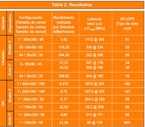 The last column of the table provides the number of real-data floating-point operations per second in units of 10⁹ (GFLOPS) for each configuration. The number of operations required by each solver depends on the decomposition algorithm used. The figures shown are obtained from the actual implementation of the Cholesky and QR solver algorithms on complex floating-point data in the two FPGAs used for this evaluation. For the Cholesky solver, the number of real-data floating-point operations is approximately the second-order term 4n³/³ + 12n², while for the QR solver, 8mn² + 6.5m² + mn is used.
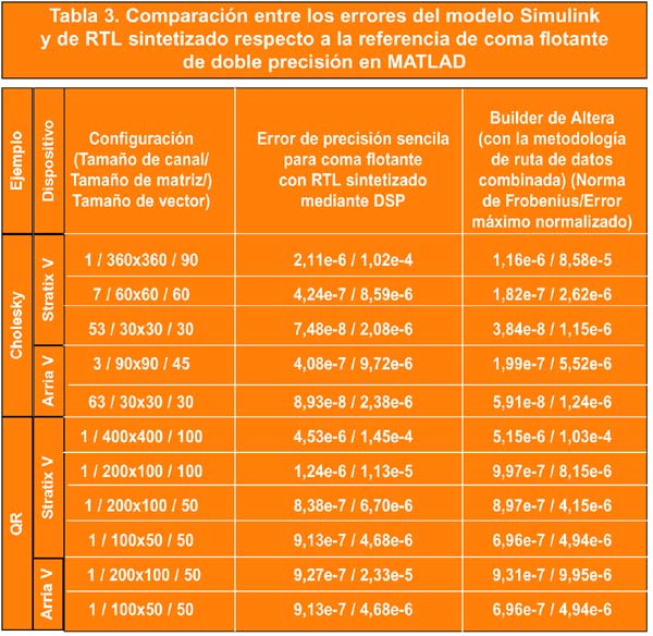
Table 3 indicates the performance of the Cholesky and QR solvers from the point of view of the error, for the simulation with Simulink and the implementation of the design using hardware development boards with single-precision floating-point operations.
The error is calculated by comparing the output of each Simulink simulation and the hardware platform with the double-precision floating-point reference for the solution vectors x generated by MATLAB. For the multichannel Cholesky solver, only the error performance of a single, randomly chosen channel is shown for brevity. Although the error depends on the input data, on average the RTL implementation leverages the combined data path methodology and achieves statistically equal or greater accuracy than the single-precision implementation of the IEEE 754 standard, as demonstrated by comparing the Frobenius norm in columns (4) and (5) of Table 3.
We use the Frobenius norm to obtain a measure of the magnitude of the total error in the resulting vector, expressed as:
||E||F = ÷SN = 0 |ei|2
i
Where N is the size of the vector, e is the difference vector between the observed x and its reference generated by MATLAB, and ei is the index of the elements in the vector e. The maximum normalized error is expressed as:
max (|(xi-obs - xi-ref)/xi-ref|)
i
5. Conclusions
This article has evaluated a new method for implementing floating-point DSP algorithms with FPGAs using the design flow of Altera's DSP Builder Advanced Blockset. This design flow incorporates Altera's DSP Builder Advanced Blockset, Altera's Quartus II software toolkit, and the Simulink simulator, as well as MATLAB and MathWorks' Simulink. This method allows the designer to work at the algorithmic behavior level within the Simulink environment. The toolkit combines and integrates the algorithm modeling and simulation stages, RTL generation, synthesis, placement-routing, and design verification within the Simulink environment. This integration streamlines development and enables rapid exploration of the design space at both the algorithmic and FPGA levels, reducing the overall design effort. Once the high-level design has been modeled and refined, the design can be synthesized and transferred to an Altera FPGA.
 To perform this evaluation, the design examples were the IEEE 754 single-precision complex floating-point Cholesky and QR solvers modeled in Simulink using Altera's DSP Builder Advanced Blockset. The largest design example evaluated was a QR solver for a 400x400 complex floating-point array with a vector size of 100. When run at 203 MHz, this example processes 162 GFLOPS. The GFLOPS values shown in Table 2 correspond to the actual implementation of the Cholesky and QR solver algorithms on a complex floating-point data format on the two FPGAs. For a valid comparison with other competing platforms, the same algorithms should be implemented on these platforms, and their performance measured. All results shown were achieved using Altera's DSP Builder Advanced Blockset without manual optimization or base planning. Starting with a high-level, block-based design in Simulink, the tool automatically segmented the design, generated the RTL code, and synthesized it to achieve usable speeds and resource utilization. The floating-point design workflow simplifies the implementation of complex floating-point DSP algorithms on an FPGA by combining the tools on a single platform. This combined data path methodology enables the implementation of complex floating-point data paths with greater performance and efficiency than previously possible.
The new method discussed in this article also requires a significant learning curve for using DSP Builder Advanced Blockset. This is especially true for designers unfamiliar with MATLAB and Simulink. The block-based design approach can pose an initial challenge for traditional hardware designers. Furthermore, to leverage the advantages of block-based design over hand-written RTL, designers must take additional steps to create the Simulink model. For example, to test different matrix and vector sizes, as demonstrated in the two design examples described in this article, the Simulink model was structured to incorporate a parameter-driven design to explore various design configurations.
Currently, designers using the DSP Builder Advanced Blockset are limited to the elements supplied by the blockset to achieve optimized performance. Elements in the standard DSP Builder Blockset are not optimized with the floating-point compiler and cannot be combined with the Advanced Blockset at the same hierarchical level. Hand-coded HDL blocks can only be imported into the Standard Blockset. Furthermore, the DSP Builder Advanced Blockset is geared towards DSP implementations and may be limited to designs that include powerful control and state machines.
The next version of DSP Builder Advanced Blockset, scheduled for release in late 2012, will include floating-point extensions. Designers will no longer be limited to the single- and double-precision IEEE 754 formats, but will instead be able to choose from a total of seven different precisions, ranging from 16 to 64 bits (exponent plus mantissa). Using the new Enhanced Precision Support block in DSP Builder Advanced Blockset, designers can select the data width that best suits their application.
Author:
By the Berkeley Design Technology, Inc. team. October 2012
6. References
[1] Berkeley Design Technology, Inc., 2011. “An Independent Analysis of Altera's FPGA Floating-point
DSP Design Flow.”
Available for download at http://www.altera.com/literature/wp/wp-01166-bdti-altera-floating-point-dsp.pdf
[2] S.S. Demirsoy, M. Langhammer, 2009. “Fused datapath floating point implementation of Cholesky decomposition.” FPGA'09, February 2009.