In the relentless pursuit of miniaturization and increased efficiency, power devices using gallium nitride field-effect transistors (GaNFETs) have become ideal candidates for overcoming these limitations. GaN is an emerging technology that promises higher power with ultrafast switching and lower switching losses. These advantages enable solutions with higher power density. The current market is saturated with a wide variety of silicon MOSFET drivers, and new GaN drivers and drivers with integrated GaN drivers are still a few years away from becoming available. Along with simple, dedicated GaNFET drivers (such as the LT8418), complex buck and boost drivers designed for GaN (LTC7890, LTC7891) are also available. A simple 4-switch buck-boost solution is not yet available. However, controlling GaNFETs is not as difficult as it might seem. With some basic knowledge, drivers designed for silicon MOSFETs can be adapted to control GaNFETs. The LT8390A is an excellent candidate, as it is a unique 2 MHz buck-boost driver with a very low dead time (25 ns) (see Figure 1). The buck-boost scheme has the sense resistor in line with the inductor and outside both hot loops, a novel feature for buck-boost drivers. This allows the driver to operate in peak current control mode in both boost and buck operating regions (as well as in the 4-switch buck-boost configuration). Although this article focuses on the 4-switch GaNFET buck-boost controller, the information can be extended to simple buck or boost drivers.
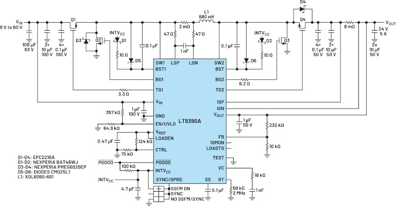
Figure 1. Schematic of the 24 VOUT and 5 A GaN buck-boost controller with 4 EVAL-LT8390A-AZ switches.
A 5V gate driver is essential
for high-power conversion. Silicon drivers typically operate above 5V, with typical silicon MOSFET gate drivers ranging from 7V to 10V or even higher. This poses a challenge for GaNFETs, which typically have an absolute maximum gate voltage of
6V. Even oscillation caused by parasitic PCB inductances on the gate and source return lines exceeding the maximum gate voltage can lead to catastrophic failures. Careful design consideration is necessary to safely and effectively drive a GaNFET, minimizing inductances on the gate and source return lines. In addition to design considerations, implementing component-level protection is critical to prevent catastrophic gate overvoltages.
The LT8390A provides a 5V gate driver specifically designed for lower gate-drive FETs, making it an ideal choice for GaNFETs. The problem is that silicon FET drivers often lack protection against accidental overvoltages. In particular, the startup supply to the upper FETs in silicon gate drivers is unregulated, meaning the upper gate driver can easily stray above the GaNFET's absolute maximum voltage. Figure 2 shows how to address this: a 5.1 V Zener diode (D5 and D6) is placed in parallel with the startup capacitor to limit that voltage to the recommended control level for the GaNFET. This ensures that the gate voltage remains within the safe operating range.
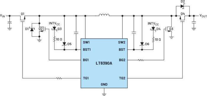
Figure 2. Simplified schematic of the 4-switch GaN buck-boost controller with GaN control protection components.
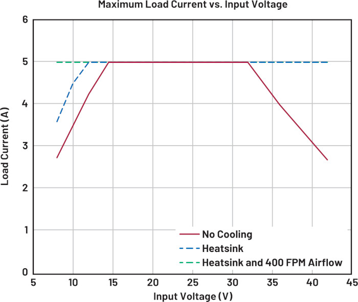
Figure 3. Maximum output current of the EVAL-LT8390A-AZ versus input voltage. The board can produce 120 W across a wide input range at high frequency.
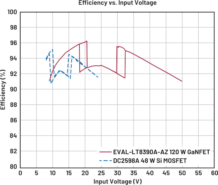
Figure 4. Efficiency of the GaN driver EVAL-LT8390A-AZ versus the efficiency of the silicon MOSFET driver DC2598A. GaNFETs provide higher efficiency at higher voltages.
Furthermore, for added protection, a 10 Ω resistor is added in series with the bootstrap diodes (D3 and D4) to reduce any oscillation that might be caused by the high-power, very-fast switching node.
Dead Time and Body Diode Challenges:
In traditional converters, there is a capture diode that conducts during the turn-off time. Synchronous converters replace the capture diode with another switch to reduce the forward conduction loss of a diode. However, a problem arises if the upper and lower switches are turned on simultaneously, causing triggering. In the event of triggering, both FETs can essentially short to ground, which can lead to component failure and other disastrous consequences. To prevent this, drivers implement a dead time, a period during which neither the upper nor lower switch is on. Typical DC-DC synchronous drivers implement dead times of up to 60 ns. This dead time is not a significant problem with silicon MOSFETs, as the body diode conducts during this period.
GaNFETs do not have body diodes and turn on and off much faster than silicon MOSFETs. Instead of body diodes conducting during dead time, GaNFETs can conduct at 2 V to 4 V, compared to the typical 0.7 V of a diode. This conduction voltage, multiplied by the conduction current, can result in a power loss almost six times greater during dead time. This increased power loss, combined with a prolonged dead time, can lead to overheating and damage to the FETs. The best solution is to minimize dead time. However, drivers intended for silicon FETs design the dead time with the understanding that silicon FETs have slow turn-on/turn-off characteristics (in the tens of ns). Therefore, the dead time is set longer to prevent triggering.
The LT8390A has a set dead time of 25 ns, which is shorter than that of many synchronous drivers on the market. While this is adequate for controlling high-frequency, high-power MOSFETs, it is still too long for GaNFETs. GaNFETs can turn on extremely quickly (in nanoseconds). Therefore, to mitigate additional conduction losses during dead time, it is recommended to add a capture Schottky diode in antiparallel with the synchronous GaNFET to divert conduction to a lower-loss path. D1 and D2 in Figure 2 show which FETs the Schottky diodes should be placed on. D1 is placed on the synchronous buck-side FET, and D2 on the synchronous boost-side FET. For a simple buck converter, only D1 is needed. For a simple boost converter, use D2.
Higher Power at Higher Frequency:
The LT8390A has a switching frequency of up to 2 MHz. GaNFETs have significantly lower switching losses compared to silicon MOSFETs, allowing for similar power losses at higher switching frequencies and voltages. The EVAL-LT8390A-AZ demonstrates the efficiency and compact size advantages of using GaNFETs by setting the switching frequency to 2 MHz.
With a 24 V output, the GaNFETs can produce 120 W of power at room temperature. The board size is comparable to the previous LT8390A evaluation board, the DC2598A, which uses silicon MOSFETs and provides a 12 VOUT output with 48 W of power.
Figure 3 shows the maximum power handling capacity of a 2 MHz GaN buck-boost, while Figure 4 compares the efficiency of both boards. Even at higher voltages and with 2.5 times the power output, the GaNFET board offers greater efficiency than the silicon MOSFET board. The use of GaNFET allows operation at higher voltages and power levels with a similar board area.
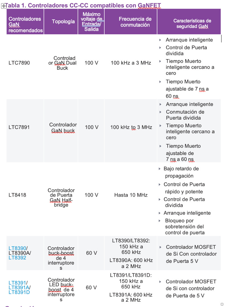
Table 1. GaNFET-compatible DC-DC controllers
Conclusion:
Even if there are no DC-DC controllers specifically designed for GaNFET control, it is still possible to control them effectively. Even using a controller originally intended for Si MOSFETs, the EVAL-LT8390A-AZ can easily outperform its power rating and achieve higher efficiency in a similar board area. Table 1 shows a wide selection of recommended controllers for GaNFETs. For even higher power requirements, such as parallel buck-boost GaNFET control, please contact the manufacturer. By researching a controller that offers a 5V gate driver and incorporating additional external protection circuitry, it is possible to control GaNFETs safely and explore further options in power conversion design.
About the author:
Kevin Thai is the applications director for Analog Devices in San Jose, California. He works in the IPS Power Products Group and oversees the isolated protection and flyback product lines, along with other boost, buck-boost, and GaN controller products. He received his bachelor's degree in electrical engineering from Cal Poly, San Luis Obispo, in 2017, and his master's degree in electrical engineering from the University of California, Los Angeles, in 2018.