


PCBs are vulnerable to mechanical shocks and thermal loads to which they are exposed during manufacturing, transport, and, of course, during use throughout their lifespan. Original equipment manufacturers (OEMs) need to identify the root causes of potential failures resulting from deformation, improper use, vibration, shock, or thermal effects.
Consequently, many OEMs and electronics suppliers conduct mechanical load tests on their printed circuit boards, in accordance with the IPC/JEDEC 9704 directive. To simplify testing during R&D or verification during production, HBK has developed a compact and scalable PCB Testing Kit, which allows for rapid deformation testing and provides accurate results on product reliability.
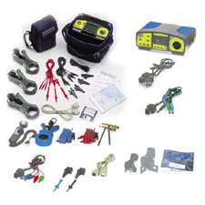
The PCB Testing Kit contains all the necessary materials: pre-wired strain gauges and their installation hardware, a QuantumX MX1615B bridge module, and catman data acquisition software. It includes a ready-to-use software project and a pre-configured test certificate in Microsoft Word format. The PCB Testing Kit uses standard products and can be replenished or upgraded at any time.
It comes with a one-year software maintenance program and free video tutorials.