Package-level integration was the first breakthrough, followed by wafer-level integration, which provides at least ten times greater connection density, a smaller footprint suitable for size-sensitive applications, and superior performance.
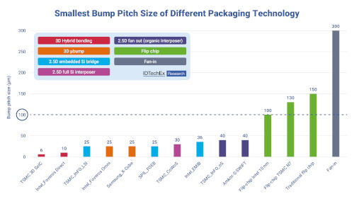
Wafer-level integration encompasses integrated circuit packaging technologies such as fan-on, fan-on-core, high-density fan-on, 2.5D, and 3D. However, only semiconductor packaging technologies with a bump pitch of less than 100 µm are considered "advanced." This includes high-density, 2.5D, and 3D integrated circuit packaging technologies.
The transition from 2.5D hybrid integration to full 3D vertical integration is crucial for future data-centric applications, and this article will focus on this transition.
The main challenge in the transition from 2.5D to 3D is scaling up the bump pitch size. In a 2.5D IC package, the bump pitch size ranges from 25 µm to 40 µm, depending on the interlayer material. However, for a 3D stackable package, the bump pitch size must be reduced to a single digit of a µm or even below 1 µm. TSMC has reported that the bump pitch for stacking N7/N6 chips is 9 µm and 6 µm for stacking N5 chips. It is expected to decrease to 4.5 µm for stacking N3 chips and continue decreasing in future generations of integrated circuits. Stacking two chips with a small bump pitch size presents a significant challenge, as high-precision alignment of the junction dielectric materials must be achieved, especially at low temperatures. Furthermore, proper control of the copper filler materials is necessary to prevent overflow during the bonding process. Additionally, thermal management becomes critical for packages with small bumping scales, necessitating package designs that allow for better heat transfer and potential liquid cooling technologies.
The engines of growth
IDTechEx has identified four main application areas for advanced semiconductor packages: high-performance computing (HPC)/data center applications, communication networks, autonomous vehicles, and consumer electronics. The increasing demand for data processing is the primary driver of growth in these application areas. However, each application has specific requirements that necessitate different advanced semiconductor packaging technologies.
For HPC applications and data centers, the priority is delivering superior data processing capacity, making 2.5DIC technologies that use silicon interpolators or silicon bridges the preferred option, despite their higher cost. In contrast, consumer electronics, such as smartphones and smartwatches, focus on miniaturization and cost, so organic-based packaging technologies are the first choice.
In 5G and later communications, the main challenge is transmission loss. Therefore, advanced packaging technologies are used to bring the antenna closer to the RF IC chip and minimize transmission loss. The "antenna-in-package (AiP)" is currently the most viable option for 5G mmWave, while the "antenna-on-chip/wafer (AoP)" continues to be intensively developed to reduce costs.
For future autonomous vehicles, the heterogeneous integration of CPUs and other components, such as HBMs and reliable power supply systems, will create new opportunities for advanced semiconductor packaging and innovation.
The expansion of data processing is the unifying factor in the growth of all these applications. However, because the requirements of each application area differ, advanced semiconductor packaging technologies are being used to meet specific needs.
Author: Yu-Han Chang, technology analyst at IDTechEx