Introduction
Data centers power the internet and connect communities around the world. Social media companies like Facebook, Instagram, and X (formerly known as Twitter) rely on data centers for information dissemination and storage, while search engines like Yahoo! and Google use data centers to power their core search engine and storage functions. Nearly every major enterprise and government agency worldwide requires reliable data center functionality to operate and maintain their core business functions through intelligent computing, storage, and search. As the number of users grows each year, data center capacity continues to expand at an extraordinary rate to keep pace with demands and technological advancements. As these growth demands increase, so too must the data center system architecture to keep up.
OCP, an organization that shares data center designs, has a system architecture definition based on Open Compute Project Open Rack Version 2 (OCP ORV2) in which the backplane voltage is nominally 12 V and the system power is 3 kW. On the other hand, increased usage leads to higher power demands, excessively raising the system's 12V power requirement and consequently impairing overall system performance. To address this issue, the backplane voltage is increased to 48V while the system power supply remains unchanged. This minimizes the amount of current traces and copper required and reduces heat dissipation in the backplane. This change improves overall system efficiency and reduces the need for a complex cooling system. This is the basis of the new Open Rack Version 3 standard, OCP ORV3.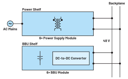
Figure 1. The OCP ORV3 power architecture.
Data center reliability is a fundamental operational requirement. Adding Battery Units (BBUs) to the system provides system redundancy. In the event of a power outage or voltage drop, the system needs time to detect the situation, preserve vital data, and transfer operations to another server within the data center, most likely in a different facility and location. This must be achieved seamlessly. Backup power systems are used in each rack to regulate the system's backup power. This requirement is defined in the latest standard, ORV3 BBU, as a power output of 15 kW, equivalent to 4 minutes of system operation per BBU, based on the energy storage and conditioning of a lithium-ion battery.
This specification provides Analog Devices with guidance for completing and designing a reference design solution that incorporates its bidirectional power converter for a single circuit dedicated to charge and discharge operation, a battery management system (BMS) device, an integrated design system host microcontroller with firmware and GUI support, and hardware amplification through collaboration with the OCP organization.
Hardware Design and Implementation Requirements
As the OCP organization provides the specification (Revision 1.3), it will outline the requirements necessary to conceptualize and design to meet the BBU module standard. The reference design of the BBU module is based on the 48 V ORV3 proposal and consists of a battery pack with a BMS, charge/discharge circuit, and other functional blocks, as illustrated in Figure 2.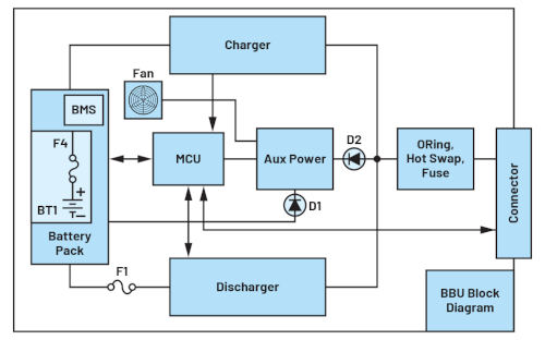
Figure 2. OCP ORV3 BBU block diagram.
Aside from circuitry requirements, the BBU module must have several main operating modes during its lifetime, which are as follows:
- Sleep mode: This occurs when the BBU module is in transit or storage, or is not connected to an active busbar, minimizing the cell's discharge current for longer storage time. BBU monitoring or reporting is not available in sleep mode. The BBU will wake up and exit sleep mode when the busbar voltage is detected to be above 46 V for > 100 ms and < 200 ms and the PSKILL signal is low.
- Standby mode: This is when the BBU module is fully charged and in good condition, and it constantly monitors the busbar voltage to be ready for a discharge event. The BBU module operates in this mode for most of its lifetime. The status and parameters of the BBU modules are visible on the upstream rack monitor via the communication bus.
- Discharge mode: When the bus voltage drops below 48.5 V for > 2 ms, the BBU module's discharge mode is activated. The BBU module is expected to restore the bus voltage within 2 ms, with a reserve time of 4 min.
- Charge mode: This is when the BBU module enables its internal charger circuit to charge the battery pack when all conditions are met. The charging current can range from 0 A to 5.5 A, depending on the previous depth of discharge of the battery capacity. The system also allows the charging current to be overridden via the communication bus. A charger timeout control scheme based on the calculated charging current must be in place.
- State of Health Check (SOH) mode: This is when the BBU module routinely checks the battery pack capacity by forcibly discharging it. The BBU module will perform the SOH test every 90 days to determine the battery's EOL status.
- System Control mode: The BBU will allow the upstream system to control the charger/discharger's operation via the communication bus.
In addition to the BBU module's operating requirements, OCP specifies the standard for battery pack capacity, battery cell type, and battery pack configuration. These are as follows:
- Battery pack capacity: The BBU module must provide 3 kW of standby power for no more than 4 minutes over a period of 4 years.
- Battery cell type: The BBU module must be of the Li-Ion 18650 type with a cell voltage of 3.5 V to 4.2 V, a minimum battery capacity of 1.5 Ah, and a continuous discharge current rating of 30 A.
- Battery pack configuration: The BBU module must have an 11S6P battery pack configuration (six parallel strings of 11 cells in series each).
In addition, the BBU module is required to have a BMS for battery charge/discharge algorithms, protections, control signals, and communication interfaces. The BMS is also responsible for providing a cell balancing circuit in which the voltage of the battery pack cells is maintained within a margin of ±1% (0.1 V).
The reference design block diagram (see Figure 3) shows the selected components and integrates various elements designated for specific tasks, creating circuits capable of providing uninterrupted power, determining module status, detecting faults, and handling module communications. The LT8228, a bidirectional synchronous controller, is housed within the BBU module. This device provides power conversion in the event of a mains power interruption and battery charging during uninterrupted operation. The LT8551, a 4-phase synchronous DC-to-DC boost converter, works in tandem with the LT8228 to increase the discharge power delivery capacity to 3 kW per BBU module. In addition to the power conversion ICs, the BBU module incorporates the MAX32690, an ultra-low-power Arm® microcontroller responsible for the overall system operation. The LTC2971, a 2-channel power system manager, is used for accurate power line fault detection and detection, as well as for a crucial voltage drop function. The MAX31760, a precision fan speed controller, was used to cool the system during charging and discharging operations. An EEPROM acts as data storage, allowing the user to retrieve any usable data from the BBU module during its service life. In addition to the power converter and maintenance microcontroller, a BMS integrated circuit was included in the design. The ADBMS6948, a 16-channel multi-cell battery monitor, is used to monitor the battery voltage level, while its inherent coulomb counter was employed to determine the state of charge (SOC) and SOH levels for cell balancing and battery lifetime calculation. The battery health monitoring procedure is performed by the MAX32625, an ultra-low-power Arm microcontroller. Both microcontrollers were carefully selected to reduce overall power consumption and thus extend battery life during BBU standby operation.
In addition to the supplied components, this reference module also manufactures and builds the BBU module (see Figure 4a) and the BBU rack (see Figure 5) to house and demonstrate the reference design according to the mechanical specifications of the OCP ORV3 BBU module and rack. The BBU rack includes six slots for the BBU module, so a single BBU rack can provide up to 18 kW of backup power as needed.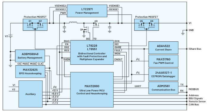
Figure 3: Block diagram of an Analog Devices OCP ORV3 BBU.
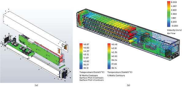
Figure 4. (a) 3D rendered mechanical overview of an ADI BBU module and (b) airflow simulations.
Mechanical representation and airflow simulation are two of the architectural advantages of the BBU module reference design. First, it includes a visualization that allows for accurate and visually appealing representations. Mechanical-structural analysis identifies design problems and potential changes at an early stage, aiding the entire design process. Last but not least, it can reduce the need for physical prototypes, which can be time-consuming and expensive. Furthermore, airflow simulation allows for performance analysis, identification of potential problems, and increased design efficiency. It also addresses thermal management, helping to identify hotspots, optimize heat loss, and improve overall system reliability. In addition, planning battery spaces to ensure safety and regulatory compliance helps reduce risks. For more information, see Figure 4b.
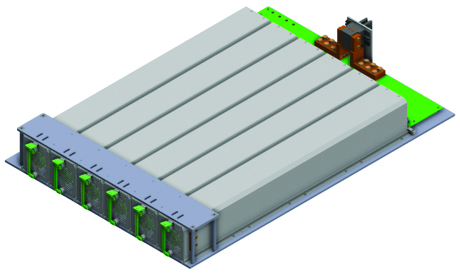
Figure 5. 3D representation of an ADI BBU rack with six BBU modules inserted.
Data and Results
The test results presented below comprise steady-state performance measurements, functional performance waveforms, temperature measurements, and operational transitions. The following configurations were tested using the BBU module reference design:
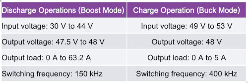
Table 1. Parameters of the ORV3 BBU module
Discharge operation (Boost mode) Charge operation (Buck mode)
Input voltage: 30 V to 44 V Input voltage: 49 V to 53 V
Output voltage: 47.5 V to 48 V Output voltage: 48 V Output
load: 0 A to 63.2 A Output load: 0 A to 5 A
Switching frequency: 150 kHz Switching frequency: 400 kHz
Performance Data:
Efficiency and Power Loss.
The reference design of the BBU module demonstrates the ability to overcome the efficiency and power loss limitations specified in the ORV3 BBU specification. The discharge and charge limitations were set at 97% and 95%, respectively. For the discharge operating period, the average efficiency measured at half load (31.6 A) was 98.5%, while the average efficiency at full load (63.2 A) was 98%. High efficiency and reduced ripple current were achieved by using a substantially larger inductor, lower drain-to-source resistance of the MOSFETs, and a carefully selected switching frequency. Furthermore, the BBU module achieves a high average efficiency of 97% during load operation with a 5 A load. Operating at a switching frequency of 400 kHz and using the same inductor value further increased efficiency and minimized power losses. High efficiency and lower power losses will extend the battery's lifespan and reduce the fan speed required for thermal cooling. See Figure 6.
On the other hand, conduction losses in the control and timing MOSFETs contribute to the overall power losses during BBU discharge and charge operations.
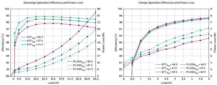
Figure 6: Efficiency and power loss during discharge and charge operating modes, respectively.
Output Voltage Drop
Another requirement of the ORV3 BBU specification was the inclusion of a voltage droop during discharge mode operation. The voltage droop is the deliberate loss of the BBU's base plate voltage during system load operation. The BBU's base plate voltage is modified in real time in response to the system load current measured by the LTC2971 in-circuit DAC converter. As a result, the base plate voltage drop from no load to full load is kept below the ±1% limit required by the ORV3 BBU. See Figure 7.
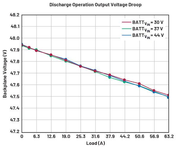
Figure 7. Output voltage droop during discharge mode operation.
Switching Waveforms:
Examining the switching waveforms provides valuable information for performance evaluation, fault analysis, efficiency optimization, EMI reduction, and safety considerations. It allows engineers to identify and resolve problems, optimize system performance, and ensure the reliable and efficient operation of the BBU module in the data center.
The switching operation of the BBU module is critical during discharge mode, as it converts the 30V to 44V battery pack voltage to a 48V motherboard voltage. This is achieved using a synchronous power MOSFET precisely regulated by the pulse-width modulation (PWM) signal of the LT8228 and assisted by the LT8551, which replicates the action of the LT8228. The switching frequency and the current distribution of each phase, resulting in a stepped voltage, are important for its operation. Figure 8 shows the switching waveforms of the main converter and its multi-phase expander under full load. In load mode, the bidirectional converter operates in single-phase mode, reducing the 49 V to 53 V input voltage from the motherboard to 44 V to charge the battery pack. It operates by rapidly switching the synchronous power MOSFET and increasing the inductor current. The switching waveform of the bidirectional converter with a 5 A load is shown in Figure 9.
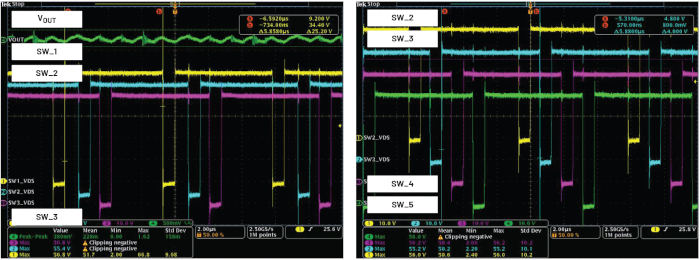
Figure 8. Switching waveforms of the main controller and expander during discharge mode operation at 44 V input and 63.2 A output load.
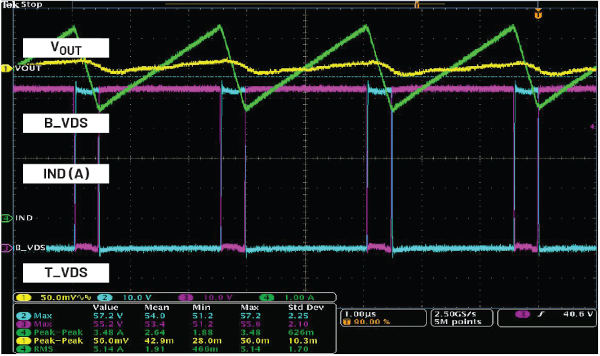
Figure 9. Waveform of a main controller during charging mode operating at 53 V input and 5 A output load.
Thermal Performance:
Thermal performance and efficiency must be carefully balanced. While it is critical to have a BBU module that can withstand high temperatures and continue operating without overheating, it is equally important to have a BBU module that can operate at optimal efficiency, converting as much input power as possible into output power. In Figure 10, the worst temperature measured on the board was only 40°C to 60°C during discharge operating mode, which operated at full load for about 4 minutes. In charge mode, the temperature on the synchronous MOSFETs was below 50°C. A properly constructed air-cooling system reduces the heat emitted by the components and prevents thermal runaway. Proper cell spacing in the battery stack and adequate airflow design provide sufficient thermal cooling. See Figure 12.
Operational Transition:
The transition operation of a BBU module is critical to ensuring uninterrupted power during power outages or fluctuations. This procedure involves the seamless transfer of power from the battery pack to a data center backplane, ensuring that vital systems and devices continue operating for 4 minutes. The BBU module constantly monitors the backplane bus voltage. When the bus voltage drops to the BBU module's activation level of 48.5 V for 2 ms, the BBU module's base plate voltage must increase to deliver full power to the bus within 2 ms. The bus voltage must never fall below the BBU module's activation level. The bus voltage must never fall below 46 V during the entire transition. Upon detecting that the bus voltage is above 48.5 V for more than 200 ms, the BBU module exits discharge mode. See Figure 12.
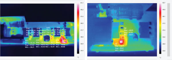
Figure 10. Thermal performance of the plate operating at full load during the discharge and charge operating modes, respectively.

Figure 11. Design of the gap of a battery stack.
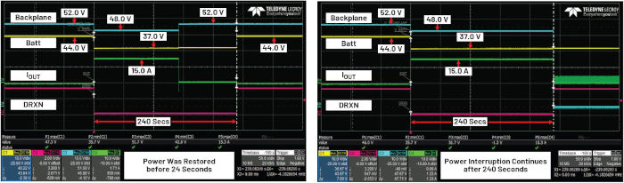
Figure 12. Transition from stable operation to power supply interruption.
Summary
Data centers are adopting 48V systems to save energy. The 48V server rack is more efficient in terms of power and heat dissipation, size, and cost than the 12V server rack due to lower current, copper losses, and the size of the power busbar. A high-efficiency, unregulated front-end stage followed by a voltage regulator tuned to the appropriate load is best suited for the microprocessors and memory in data center servers. Such levels of reflection, along with the latest innovation from OCP, pave the way for more efficient power distribution and intelligent battery backup unit design to support continuous, fault-free operations.
Selecting and implementing the right device for the BBU module and bracket simplifies the overall design, extends battery lifecycle, reduces lengthy engineering development time, and minimizes engineering and production costs. Furthermore, providing mechanical simulations shortens the prototyping phase, offers data that can be used to improve cooling and thermal management, and increases design reliability. Finally, providing a suitable and well-designed algorithm and firmware sequence ensures smooth and effortless operation of the BBU.
The second part of this series will review the main functions and operations of the microcontroller in the various BBU modules in relation to their specialized design for BBU maintenance. It will also provide a deeper understanding of how useful information is monitored and used to build and execute a proper workflow routine.
About the author:
Christian Cruz is a Senior Application Development Engineer at Analog Devices, Inc., Philippines. He holds a degree in electronic engineering from the University of Oriente in Manila, Philippines. He has over 12 years of engineering experience in the fields of analog and digital design, firmware design, and power electronics, including the development of power management ICs, as well as AC-to-DC and DC-to-DC power conversion. He joined ADI in 2020 and is currently supporting power management requirements for cloud-based computing and system communications applications.
Gary Sapia holds a Bachelor of Science in Engineering from Texas A&M University, with advanced coursework in power electronics and RF system design. He has over 28 years of experience focused on the design and development of analog systems, including power conversion and high-frequency solutions for the communications and GPS markets. Prior to joining Analog Devices, Gary spent 18 years as a field applications engineer at Linear Technology (now part of ADI), focusing on Cisco and other leading Bay Area networking companies.
Marvin Neil Solis Cabueñas graduated with a Bachelor of Science in Electronic Engineering from De La Salle University in Manila, Philippines. Before joining ADI in 2021, Marvin worked as a Systems Engineer for Azeus Systems Philippines, Inc., then as a Network Engineer for Technistock, Philippines, Inc. from 2014 to 2017, and as a Research and Development Engineer for Nokia Technology Center Philippines from 2017 to 2020. He has over ten years of work experience in various fields, including embedded systems programming, digital signal processing, simulation modeling, and others. He currently works as a Senior Software Systems Engineer on several projects for ADI's Energy Business Unit. He is currently pursuing a Master of Science in Electrical Engineering at the University of the Philippines.