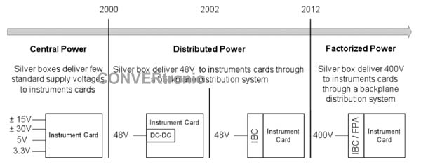
 Given the increased number and diversification of channels and loads required by instrumentation boards, distributed power supply architectures became essential. A simpler, centralized, and somewhat bulky power supply device provided a single regulated DC voltage, typically 48V, to a backplane distribution system. Test boards dedicated a portion of their surface area to DC/DC converters, usually on their periphery, and their outputs closely matched the needs of the measurement circuits.
Test circuitry now demands more power to operate, and its voltage/current requirements cover a wide range of values. At the same time, test instruments not only need power but also the ability to precisely and quickly modulate multiple voltage rails to fully characterize the analog partitions of a device under test. The power supply system is becoming a key component of the ATE (Analog Test Equipment) due to the increasing performance and density levels of the most advanced VLSI (Very Large Scale Instrument) or SOC (System on a Compute) designs.
The trend towards "higher density" and "higher dynamics" is also complex at voltages within the 48V range, as higher currents require larger copper cross-sections on boards with higher device density. New concepts such as factored power architecture and 400V DC distribution are currently being explored.
Next, we will analyze how the requirements of the instrumentation cards and the devices under test affect the distributed power architecture in the ATE system, and the main design parameters to consider in order to optimize the distribution network in the ATE rack, between several instrumentation cards and up to the measurement circuitry.
Considerations Regarding Distributed Power Network Design
As noted in the previous paragraph and as shown in Figure 2, centralized power supply has been largely abandoned, and distributed power supply with backplane distribution is the most widespread practice today. The telecommunications and data communications sectors have long used this technique and, in many respects, face the same challenges as a modern ATE. In fact, many of the silicon chips that ATEs need to verify and characterize are implemented in telecommunications, computing, and routing systems used by the telecommunications sector to move an increasing volume of data over wired and wireless networks worldwide. The most striking similarity between these two "worlds" is the need for dense and granular power supply systems, albeit with different objectives: performance and flexibility for ATEs, and total cost of ownership for telecommunications and data communications systems.
Design considerations from a systems perspective.
Bill of materials
. Objective: to minimize the bill of materials.
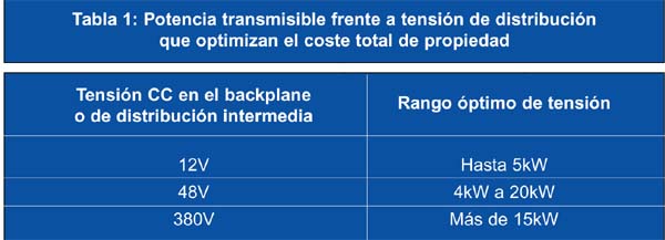
The bills of materials for distributed power supplies are directly affected by one main parameter: the distribution voltage on the backplane. Simply considering distribution losses should determine the choice of copper cross-section. The primary concern for ATEs (Analog-to-Earth Testers) is to avoid thermal problems; therefore, distribution losses should be kept within a range easily manageable by the existing cooling system. Furthermore, if it is necessary to connect the instrument boards while they are fully operational, appropriate OR-ing devices should be installed on each board. Table 1 provides guidance derived from studies conducted in telecommunications data centers. While ATEs requiring more than 20kW are only those that support high levels of parallel testing, it is clear that 48V backplanes are likely no longer the best option, and greater utilization of 400V backplanes, with their lower currents, is expected when 48V is insufficient.
Operating Costs, Efficiency and Losses, Thermal Management.
Objective: To optimize the thermal management system by controlling distribution losses.
Up to now, we have focused on backplane distribution. While thermal management on the backplane is not usually too difficult, controlling the instrument board's power supply system can be quite complex. Furthermore, the power buses on instrument boards occupy valuable space on the board itself. Therefore, the most logical choice is to distribute the backplane voltage on the board as close as possible to the load, whether it be the measurement circuitry or an integrated DC/DC converter. Naturally, if a low voltage is used on the backplane—for example, 12V—the copper on the printed circuit board should not only be the correct size but also have adequate cooling.
A less obvious aspect is the difficulty of accurately compensating for DC (I²R) and AC (L·di/dt) voltage drops as current levels increase. Designers may need to oversize the converter's power components and add filtering and decoupling networks for distributed supply voltages below 48V.
Flexibility and Granularity
Objective: To allow the maximum degree of flexibility in the design and configuration of the test board.
Instrument boards must supply an ever-increasing variety of loads. Therefore, power supply systems with granular components provide a considerable advantage to the designer. One effective solution is to adopt an intermediate bus architecture, in which the backplane voltage is effectively reduced to a lower, “intermediate” bus voltage and then regulated by a standard-type synchronous step-down converter at the load point.
Within the flexibility paradigm, reusing a design has become a common option to leverage standardization across various power systems. Designers can "acquire and customize" numerous regulators from a pool of valid designs to suit specific electrical loads and place them as close as possible to the loads themselves to maximize dynamic performance. Groups of regulators would be powered by a single intermediate bus with the support of a bus converter. While good design practice would involve matching the converter's power output to the needs of the downstream regulator, there are typically constraints on the effective distribution of the intermediate bus "on the board." For an intermediate bus voltage of 12V, distributing even as little as 300W involves driving 25A, which can be challenging in high-density designs.

Reliability and Redundancy
Objective: To achieve maximum system availability through design that enhances reliability and redundancy.
The distributed power supply network is the backbone of complex equipment, power measurement systems, and devices under test. Since the operational life of an ATE (Assisted Distribution Equipment) is typically measured in decades, it is necessary to identify and monitor the mean time between failures (MTBF) of critical components. This includes:
Appropriate speed reduction from an electrical and thermal point of view – While speed reduction is generally considered a way to reduce thermal stress, current density can also be helpful in understanding failure mechanisms. An example is electromigration on printed circuit board traces.
Redundancy – Critical components whose failure affects machine availability should be redundant, and spare parts should be available for on-site replacement.
Repairability and Diagnostic Telemetry
Objective: To enable the highest level of modularity and provide the system with online diagnostic options throughout its lifecycle.
The backplane distribution technology is inherently very flexible, allowing for the full-operation swapping of non-critical loads (such as fans) that can be replaced on-site while the equipment remains operational. However, the same level of flexibility should be planned for the other end of the distribution network, thus facilitating access to the bulky power supply system.
Diagnostics also becomes a critically important aspect. It is necessary to quickly identify and isolate problems with components or subsystems to protect the system from propagating faults. While nearly impossible with centralized power architectures, both distributed and factored power architectures offer a way to automate distributed power network diagnostics. Distributed power architectures traditionally use a "margining" technique, in which the remote DC/DC converter is controlled by a pre-established sequence, and a dedicated power network verifies the resulting dynamic DC or AC output. Modern power components and factored power architectures offer a simpler digital interface where supervisory controls can request real-time status information via a serial interface bus, typically I2C or UART.
Noise Sources and Immunity
Objective: To minimize EMC and EMI within the system by decoupling the distributed power network to minimize conducted and radiated interference.
EMC and EMI are commonly considered the "black magic" of power design. However, a number of basic rules generally apply. First, identify the noise source; and second, contain or filter the noise as close to the source as possible (assuming the noise cannot be completely avoided). Unfortunately, the distributed power network is a prime candidate for distributing conducted noise within the system as well as radiated noise around the system rack. Therefore, it is extremely important to implement appropriate filtering, if not at the level of each DC/DC component, at least at each instrument card, in order to prevent crosstalk in the backplane.
A particularly troublesome problem is the low-frequency noise generated in the backplane as well as on the intermediate buses. This is due to interactions between the input currents of various converters, creating low-frequency beats. Designers can try to avoid this problem by ensuring that all switching current components are sufficiently confined within each converter.
Conclusion:
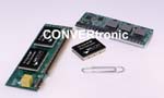
The design of a distributed power network presents a challenge for even the most advanced testing systems. Several aspects must be carefully evaluated in the chosen power system architecture. While distributed power architectures based on 48V backplanes are currently the most common option, advanced architectures such as factored power from a 400V DC distribution are becoming increasingly valuable as they improve system density by offering greater efficiency and a higher level of granularity. The figure shows an example of a standard two-stage design for powering the point of load from a 400V DC distribution: on the left, an input module consisting of two 400V bus converters (beneath the heat sinks, and a single module shown near the clip); at the top, a multi-phase voltage regulation module (VRM) with the classic 12V buck converter.
Author:
Maurizio Salato, Director of Systems Engineering, VICOR