Power DC-DC switching converters are notorious for physically disrupting the circuitry of a supposedly carefully designed system. Specifically, these power converters conduct unwanted loads to ground (GND), resulting in erroneous digital signals, double flip-flop timing, electromagnetic interference (EMI), analog voltage errors, and damaging high voltages. This article explains the two main sources of ground noise and offers suggestions for reducing it in both sources.
Problem 1: Ground Noise.
Figure 1 shows an ideal buck converter with a constant load current. Switches t1 and t2 open and close, cutting off the Vin voltage through the Lbuck and Cbuck circuits. Neither the inductor current nor the capacitor voltage can change instantaneously, and the load current is constant. As expected, all switching voltages and currents pass smoothly through Lbuck or Cbuck, respectively. An ideal buck converter produces no ground noise.
However, experienced designers know that buck converters are a notorious source of noise. This fact implies that important physical elements are missing from Figure 1.
Any movement of charge generates a magnetic field. Any current in a wire, resistor, transistor, superconductor, and even any plate-to-plate displacement current in a capacitor creates a magnetic field. Magnetic flux, FB, is the magnetic field, B, passing through a current loop area, A, and is equal to the product of the field cutting the loop's surface at a right angle: FB = B·A. The magnetic field surrounding the wire at a distance r is directly proportional to the electric current in the wire: B = m₀I/2πr.
Electrical components have a length, and the charge must pass from one device to the next through the different segments of the wire. However, the moving charge generates a magnetic field; therefore, the diagram in Figure 1 can be improved. Figure 2 shows a better model of a simple step-down converter.

In Figure 2, the wire remains ideal in all respects, except that the current has to travel some distance in each segment as it passes from one electrical component to the next. As this charge flows, a magnetic field is generated around the electrified wires, and the magnetic flux passes through the loops of switches t1 and t2.
Changes in the current loop areas t1 and t2 are the primary source of ground noise in the switching converter. The magnetic flux in the Vin-t1-gnd loop increases and collapses with each switching cycle. This changing flux induces a voltage in all parts of the loop, including the ideal ground return line. This induced voltage cannot be eliminated by any amount of copper, not even a superconductor. The only solution is to reduce the changing magnetic flux.
In changing magnetic flux, three factors are distinguished: the rate of change, the magnetic field strength, and the loop area. Since clock frequency and maximum output current may be design requirements, minimizing the loop area becomes the best solution.
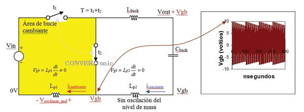
Inductance is proportional to magnetic flux; therefore, Figure 3 shows an electrical model for Figure 2 in which the changing current in the parasitic inductor Lp1 causes ground noise, unlike the constant current in the parasitic inductor Lp2.
Although Figure 3 presents the problem in an easily understandable way, it cannot satisfactorily replace the physical model shown in Figure 2. Figure 3 shows the voltage induced by the parasitic inductors Lp1 and Lp2, whereas in reality, the voltage is induced anywhere in a loop with changing magnetic flux. However, this circuit element scheme will still serve to show how induced ground noise should be reduced.
As shown in Figure 3, the ground return current circulates and changes in Lp1, causing voltage oscillation. However, by carefully positioning the input capacitor, as shown in Figure 4, the parasitic magnetic flux area is reduced, and the changing current from the reducer is directed along a path that bypasses the ground return.
In this case, the current in the parasitic inductors Lp1 and Lp2 is constant; consequently, the ground voltage will be stable. Furthermore, reducing this magnetic flux area proportionally reduces EMI and all other unwanted induced loop voltages, as demonstrated by the model in Figure 3.
In summary, the primary source of ground noise in switching converters results from changes in the magnetic flux area. A good printed circuit board (PCB) design routes traces and carefully positions the bypass capacitor to minimize changing current loop areas and the fluctuating current in a ground return path.
Ground Noise Problem 2:
The second major ground noise problem, as shown in Figure 5, results from the parasitic inductor capacitance.
Voltage cannot change instantaneously across a capacitor, nor can current change instantaneously across an inductor. Therefore, voltage changes at node LX are directly related to both the parasitic buck inductor capacitance, CL, and the filter buck capacitor, Cbuck, appearing in the parasitic ground inductors Lp1 and Lp2.

Initially, no charge flows, but after a short time, current accumulates in all these components until the energy stored in the parasitic step-down inductor capacitor, ECL = 1/2 CLVLX2, is transferred to the parasitic magnetic field of the wire, ELp = 172 Lpi2cambiante_max (where Lp is the sum of all the parasitic inductors in the loop). Then, like a back-and-forth motion, the unwanted energy oscillates between the electric and magnetic fields until it is dispersed or dissipated by the resistive elements, which are not shown in Figure 5.
Both the peak voltage and the duration of a ground noise oscillation are problematic. The peak voltage, measured at node Vgb, is a function of the voltage change at node LX, the parasitic buck inductor capacitance (CpL), and the additional parasitic trace capacitance (not displayed). A large CpL stores more energy, so less is more. After selecting the inductance and current rating of the buck inductor, an inductor with the highest self-resonant frequency should be chosen to limit the CpL capacitance.

The self-resonant frequency of an inductor is: fselfresonance = 1/[2π ÷ (LbuckCL)].
It should be noted that doubling the self-resonant frequency reduces the parasitic inductor capacitance and, consequently, the ground noise energy by a factor of four.
If performance is more important than cost, it is advisable to maintain the same inductance value by replacing the single Lbuck inductor in Figure 5 with two inductors connected in series, each having half an Lbuck, as shown in Figure 6. For a manufacturing series of inductors, the parasitic capacitance is usually proportional to the nominal inductance; therefore, half the inductance results in half the parasitic capacitance. When inductors are connected in series, their values add up and increase the inductance, but the parasitic capacitors are added as the inverse sum of reciprocals to decrease the total parasitic capacitance. In the case of a series connection of two 1/2 Lbuck inductors, the total inductance will be Lbuck_new and the total parasitic capacitance will drop by a factor of 4 to 1/4 CL.

This reduction in the parasitic inductor capacitance will in turn reduce the oscillation of the mass level, as shown in Figure 6.
Author:
By Jeff Barrow, Director of Analog IC Design, Integrated Device Technology, Inc.
Information about the author
Jeff Barrow works for Integrated Device Technology, Inc. in Tucson, Arizona, as Director of Analog IC Design. His responsibilities encompass the development and usability of power integrated circuits as well as the design of analog integrated circuits. He holds a Bachelor of Science in Electrical Engineering from the University of Arizona (Tucson), and his personal interests include geology, astronomy, physics, and electronics.