However, 650 V SiC MOSFETs offer excellent performance with a competitive RDS(ON)*Qg figure of merit and minimal reverse recovery load. This makes SiC an excellent alternative to silicon MOSFETs in hard-switchingsuch as totem-pole power factor correction (TPPFC) or synchronous boost. Some engineers believe that SiC is unsuitable for high-frequency applications and that GaN should be used instead for fast switching. However, recent technological advances have reduced the SiC die area, further increasing its suitability for high-frequency operation (>100 kHz). As a result, SiC devices are now successfully used in applications such as 100 kHz TPPFC and soft-switching at frequencies between 200 and 300 kHz. Furthermore, emerging technologies such as trench and cascoded SiC MOSFETs will further improve their high-frequency performance. Finally, other engineers believe that SiC is a niche technology based on its success in traction inverters for electric vehicles. However, the need for higher power density and efficient operation in almost every sector means that the advantages of SiC can also benefit a wide range of less complex designs, such as EV on-board chargers (OBCs), photovoltaic (PV) solar modules and renewable energy applications, as well as cloud computing.
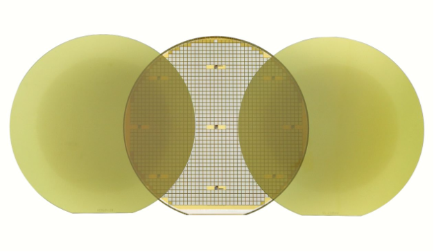 Figure 1: Image of a SiC wafer
Device Selection and Operation:
Many designers use a negative turn-off gate voltage to prevent SiC devices from "bouncing" or inadvertently turning back on due to switching transients, but this is not a strict requirement. Many successful SiC designs do not have a negative gate voltage. However, as with all designs, good practices should be followed, such as a tight design that minimizes parasitic effects. Additionally, the gate driver must be able to draw enough current to keep the device firmly off. A junction-isolated gate driver may be acceptable in a limited number of applications, such as TPPFCs. However, it should be noted that galvanically isolated gate drivers offer greater noise immunity and can better handle dv/dt transients from the switching node, preventing false triggering. Because SiC MOSFETs switch quickly and have a lower gate charge (Qg) than equivalent silicon devices, a galvanically isolated gate driver provides a more robust design, even in applications where it is not strictly required. Many modern SiC drivers offer practical features such as negative gate drive, DESAT, OCP, OTP, and other protections. Selecting the right gate driver makes controlling a SiC device no more difficult than controlling a silicon MOSFET.
Economics, Ecosystem, and Supply Chain of SiC:
There is a misconception that SiC solutions are expensive. Compared to silicon MOSFETs, the price of a SiC device is slightly higher; however, let's consider a typical 30 kW silicon-based power solution. Here, 90% of the total cost is in the inductors and capacitors (60% and 30%, respectively), and the semiconductor devices represent only 10% of the total bill of materials (BOM) cost. Suppose the silicon MOSFETs are replaced with SiC switches. In that case, the capacitance and inductance will be reduced by 75%, a significant cost (and size) reduction that offsets the increased cost of the switching components. Furthermore, silicon devices offer lower efficiency than SiC devices, thus requiring expensive and bulky heat dissipation solutions. Consequently, the total bill of materials cost of a SiC solution is lower than that of a silicon equivalent.
Economics, Ecosystem, and Supply Chain of SiC:
There is a misconception that SiC solutions are expensive. Compared to silicon MOSFETs, the price of a SiC device is slightly higher; however, let's consider a typical 30 kW silicon-based solution. Here, 90% of the total cost is in the inductors and capacitors (60% and 30%, respectively), and the semiconductor devices represent only 10% of the total bill of materials (BOM). Suppose the silicon MOSFETs are replaced with SiC switches. In that case, the capacitance and inductance will be reduced by 75%, a significant cost (and size) reduction that offsets the increased cost of the switching components. Furthermore, silicon devices offer lower efficiency than SiC devices, thus requiring expensive and bulky heat dissipation solutions. Consequently, the total BOM cost of a SiC solution is lower than that of a silicon equivalent.
The SiC ecosystem is evolving rapidly as the technology becomes more mainstream. A wide range of SiC devices and associated gate drivers are currently available, with various package types to suit diverse applications. The SiC knowledge base is expanding across the industry as manufacturers increase their support through application engineering teams, reference designs, application notes, simulation models, and tools. Component availability (not just SiC) has recently been a challenge for some sectors. However, following the recent acquisition of GTAT, onsemi's supply chain is now significantly more robust. onsemi is the only large-scale supplier with end-to-end SiC supply capabilities, including SiC boule, substrate, epitaxial fabrication, device manufacturing, best-in-class integrated modules, and discrete package solutions. To support the projected growth of SiC in the coming years, onsemi plans to quintuple the company's device and module manufacturing capacity, effectively doubling it across all production sites by 2023. And again, it will nearly double its capacity in 2024, with the potential for further growth as needed.
 Figure 2: Onsemi's end-to-end supply chain
High-Temperature and High-Voltage Robustness:
Wide-bandgap (WBG) semiconductors provide greater robustness against avalanches in SiC MOSFETs because the thermally generated concentration is much lower than in silicon devices. While it is true that SiC devices have smaller geometries, resulting in a shorter short-circuit withstand time compared to an IGBT, the use of a suitable SiC gate driver ensures fault detection and device shutdown with ample margin, allowing them to be used with confidence in robust applications. The battery voltage of many electric vehicles is increasing from 400 V to 800 V or even 1,000 V. In photovoltaic (PV) solar systems, the input voltage is rising from 600 V to 1,500 V. To meet this demand for devices with higher breakdown voltages, onsemi has developed a range of EliteSiC M1 1700 V planar MOSFETs optimized for fast-switching applications. Alongside these MOSFETs, it has also launched a range of 1700 V SiC Schottky diodes.
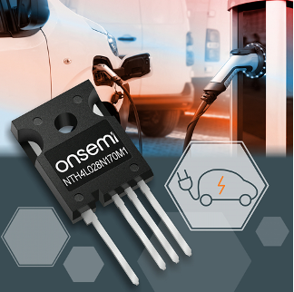 Figure 3: EliteSiC M1 1700 V planar MOSFET
Conclusion
Once silicon and silicon carbide devices have been analyzed through various metrics, it becomes clear that many widespread misconceptions lack a real basis, and that engineers should have confidence when selecting and applying this versatile technology in their designs.
Author: Ajay Hari, Director of Applications, onsemi