



The totem-pole PFC (TP-PFC) topology has been discussed in numerous articles in the past, e.g., in this journal in [1]. With the availability of WBG semiconductors incorporating high-performance body diodes, this topology is becoming increasingly attractive. Its key advantage over traditional boost-type PFC lies in eliminating low-frequency rectification and the power loss associated with the forward voltage drop of a 50 Hz rectifier. Efficiencies above 98% can therefore be achieved, and by using a suitable secondary stage with similar efficiency, the desired efficiency of 80+ Titanium can be reached.
Figure 1 shows, along with some of the design specifications, an image of the exposed evaluation kit (EVK) implementing the TP-PFC with a nominal input current of 16 A. The key devices used on this board are highlighted in Figure 1. In addition to 4th generation SiC MOSFETs, this design employs ROHM Si SJ MOSFETs, as well as the BM61S41/BM61M41 gate drivers and other ROHM components, such as the shunt resistor and the flyback switching regulator integrated circuit (IC) in the auxiliary power supply.
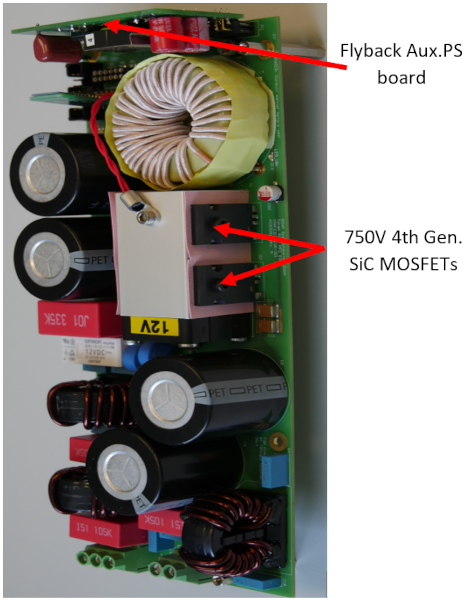
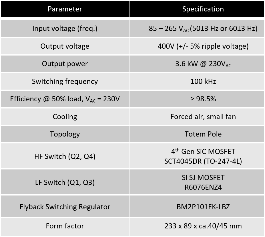
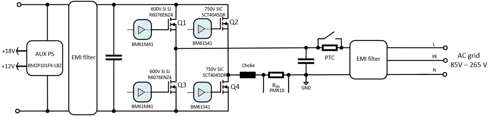
Figure 2: TP-PFC circuit diagram.
The performance of the developed EVK is illustrated in the following graphs showing the measured efficiency and the input power factor achieved at both the 230 V and 115 V AC inputs.
 Regarding efficiency, it should be noted that it includes all onboard power consumption corresponding to the auxiliary power supplies for the gate drivers, low-voltage electronics, and the fan. It can be seen that the requirement of a power factor > 0.95 is achieved with a 20% load. If the PFC circuit is combined with a suitably high-efficiency DC/DC stage, the design can also meet the efficiency requirements of 80+ Titanium.
a) Measured efficiency b) Measured power factor
Figure 3 - Measured efficiency and power factor
The following paragraphs discuss how this design was developed and how certain challenging aspects of this topology were addressed. These challenges include:
• Finding the correct settings for dead time and suppression.
• Safe auto-start at the universal mains input voltage.
• Soft start around the AC zero crossing to minimize current spikes.
The advantages of ROHM's 4th generation SiC MOSFETs will be highlighted first.
ROHM's 4th Generation SiC MOSFETs:
The new SiC MOSFETs achieve a significant 40% reduction in on-state resistance per unit area compared to 3rd generation SiC MOSFETs. This reduction is achieved without sacrificing short-circuit robustness, giving the new devices exceptional robustness and high performance.
Furthermore, switching losses in the 4th generation SiC MOSFETs are 50% lower than in the 3rd generation thanks to a drastically reduced gate-drain parasitic capacitance (CGD). This results in higher conversion efficiency.
a) Reduction in on-state resistance in 4th generation SiC MOSFETs. b) Comparison of switching losses between 3rd and 4th generation SiC MOSFETs.
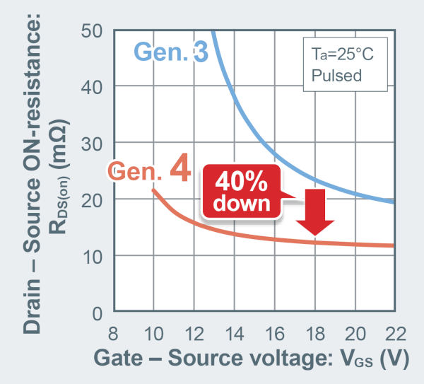 Figure 4: Reduction of switching loss and on-state resistance in ROHM's 4th generation SiC MOSFETs
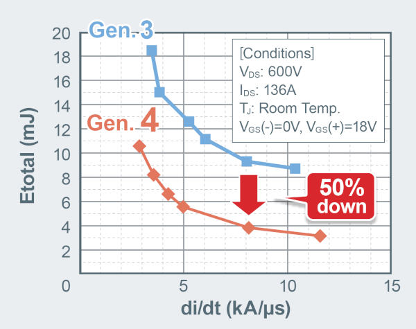 To drive the gate, in contrast to the 18 V gate-drain voltage (VGS) required in 3rd generation and earlier SiC MOSFETs, the new products support a more flexible gate voltage range (15-18 V). Furthermore, due to the reduction in parasitic capacitance (CGD) and, consequently, the CGS-to-CGD ratio, 4th generation SiC MOSFETs can be safely turned off at as little as 0 V without any parasitic connection that might be caused by a high dVDS/dt. As a result, the gate driver circuit can be simplified by eliminating the need for a negative bias for turn-off.
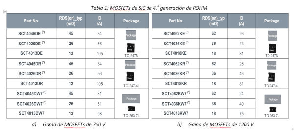 Table 1 shows ROHM's range of 750 V and 1200 V 4th generation SiC MOSFETs. The devices are available in THD (through-hole) TO-247N and TO-247-4L versions, as well as SMD (surface-mount) TO-263-7L versions. Automotive qualification is planned for all devices marked with an asterisk (*).
a) 750 V MOSFET range b) 1200 V MOSFET range
Table 1: ROHM 4th generation SiC MOSFETs
Dead Time and Suppression Configuration:
Errors associated with AC zero-crossing detection, as well as parasitic elements in MOSFETs, must be considered when configuring PWM (pulse-width modulation) control. In this TP-PFC EVK, a 50 µs suppression time has been inserted around the AC zero-crossing. During this time, all four switches are turned off shortly before the zero-crossing, either positive to negative or negative to positive, to prevent shoot-through. The control loop is paused during this time to prevent integrator buildup from causing an unwanted high-current spike by applying a large PWM pulse on the next turn-on. A short suppression time allows for greater control over the current waveform, a lower THD (total harmonic distortion), and relatively higher efficiency. However, the minimum suppression time is limited by the controller's sampling rate and the line frequency.
In addition to the suppression time around the AC zero crossing, an appropriate dead time must be set between the control commands of the complementary SiC MOSFETs. From the BM61S41 gate driver datasheet, the propagation delay has a maximum value of 65 ns. Adding another 10 ns max. for the PWM propagation mismatch results in an absolute minimum dead time of 75 ns. To account for the turn-on and turn-off delays of the SiC MOSFETs and to allow for some margin, the dead time for this board has been set to 150 ns. Naturally, this needs to be evaluated for each design and is also affected by the selection of turn-on and turn-off gate resistors.
Automatic startup on a universal mains input:
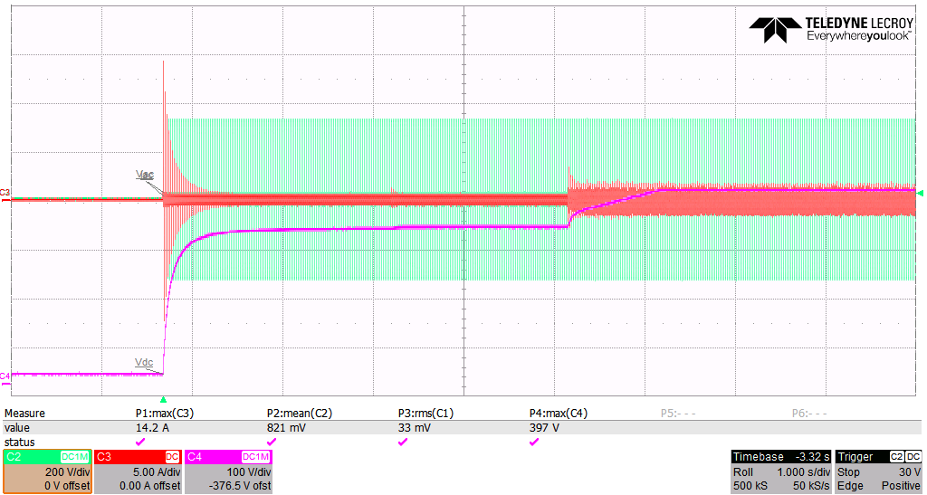
The TP-PFC EVK comes equipped with a PTC for pre-charging in parallel with a shunt relay. Upon startup, the relay is disconnected, and the large capacitors are pre-charged via the PTC to a safe threshold before the relay is connected and the converter is operated. This prevents damage to the circuit due to high inrush currents. The EVK has been tested across the entire universal input range [85 Vac-265 Vac], proving safe for automatic startup even at 265 Vac. Thanks to the implemented Second-Order Generalized Integrator Frequency Closed Loop (SOGI-FLL), this EVK can also track and detect deviations in the mains frequency of 50±3 Hz or 60±3 Hz.
a) Automatic startup 110 Vac, 400 Vdc b) Automatic startup 230 Vac, 400 Vdc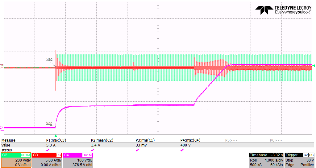 Figure 5: Automatic startup PFC vs. AC Input Voltage
Measures to Minimize Current Spikes After AC Zero Crossing
In TP-PFC topology, the MOSFET switching sequence is of crucial importance. Failure to understand or observe the control challenges in a TP-PFC can lead to improper operation, unexpected EMI problems, or even power device failure. The most common challenge inherent in this topology is the occurrence of current spikes at the AC zero crossing [2],[3]. These are primarily caused by the output parasitic capacitor “COSS” and the associated reverse recovery charge “Qrr” of line-frequency switched MOSFETs, which only change state at the AC zero crossing.
 A detailed analysis of AC current peaks and waveforms in a TP-PFC topology is presented in [2].
In ROHM's TP-PFC EVK, a soft-start sequence is implemented after each AC zero crossing. This involves increasing the duty cycles applied to the high-frequency SiC MOSFETs (Q2, Q4) and precisely controlling the switching of the low-frequency Si SJ MOSFETs. Implementing this soft-start sequence resulted in significantly lower current peaks. The implemented MOSFET switching sequence is shown in Fig. 6.
 Figure 6: Soft Start of MOSFETs in TP-PFC
. MOSFETs Q2 and Q4 are complementaryly switched. During the negative half-cycle, MOSFET Q2 is the active switch, controlled by the calculated duty cycle “D”. During this time, MOSFET Q4 operates in synchronous rectification mode with a duty cycle of “1-D”. Note that MOSFET Q1 switches only to the mains frequency and remains on for the entire negative half-cycle to provide a low-impedance return path to the mains. Operation is reversed during the positive half-cycle, and the high-side and low-side MOSFETs in each branch exchange functions.
As the input voltage changes polarity from negative to positive half-cycle, and just after the AC zero crossing, the soft-start sequence of MOSFET Q4 is activated. This sequence involves applying a boost factor to the pulse width, gradually increasing the turn-on time of this MOSFET from 0% to 100% of the calculated "D" cycle. While this is happening, MOSFET Q1 undergoes full reverse recovery, and the "VDS" of Q3 drops to ground. This eliminates the positive current spike caused by the slow recovery of Q1 and the high "VDS" voltage across MOSFET Q3.
Since the AC voltage is very low just after the zero crossing, and the inductor is already charged with the DC bus voltage, a large negative reverse current flows through the inductor back to the mains. This results in a high negative current spike when the synchronous MOSFET Q2 is turned on, even during a "1-D" duty cycle. Therefore, once Q4 reaches a full “D” cycle, soft starting is also applied to the synchronous MOSFET Q2 to reduce this negative peak to almost zero. Simultaneously, when Q2 is soft starting, Q3 must be turned on to provide the return path to the power grid.
A high negative current peak will also appear at the AC zero crossing if MOSFET Q3 turns on too late after the soft starting of Q2 is complete, as detailed in [2].
Experimental Results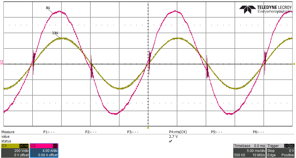 Figure 7 shows the inrush current waveform around the AC zero crossing with and without soft starting.
a) Traditional control without soft start b) With soft start method
Figure 7: AC zero-crossing inrush current spikes with and without soft start method
(red: ICA, green: VCA)
Note that, since "1-D" is very low when Q2 is first turned on, it becomes even smaller and tends to zero when multiplied by the soft start factors. Depending on the gate driver used, Q2 may remain off for a couple of PWM cycles until the term "1-D" becomes greater than the minimum PWM turn-on time of the gate driver. This results in a residual but very low positive and negative current spike at each AC zero crossing. The MOSFET control sequence explained in the previous section was implemented and tested on the 3.6 kW TP-PFC EVK. Based on the test results, without this control method, both positive and negative current spikes are present. Applying soft-start technology to both active and synchronous MOSFETs, along with precisely timed activation of the low-frequency MOSFETs, has resulted in improved current waveforms and a significantly lower THD.
In summary
, the TP-PFC EVK presented here demonstrates high performance in key design aspects, including control characteristics and high efficiency, achieving 98.5% while including all onboard power consumption from auxiliary power supplies and the fan. Both the low on-state resistance and low switching loss of the 4th generation SiC MOSFETs have contributed to achieving such performance. The results demonstrate the suitability of these new products for numerous energy conversion applications such as, for example, server and data center power supplies, telecommunications and industrial power supplies (SMPS), energy storage systems, as well as inside electric vehicles (e.g. OBC) where high power density, efficiency, simple gate circuits and short-circuit robustness are required.
References:
[1] Christian Felgemacher, Aly Mashaly “SiC Based Totem Pole PFC for Industrial Power Supplies”, Bodo's Power Systems, February 2020.
[2] Bosheng Sun, Analog Application Journal “How to reduce current spikes at AC zero-crossing for totem-pole PFC” Bosheng Sun, https://www.ti.com/lit/an/slyt650
[3] L. Xue, Z. Shen, D. Boroyevich and P. Mattavelli, "GaN-based high frequency totem-pole bridgeless PFC design with digital implementation," 2015 IEEE Applied Power Electronics Conference and Exposition (APEC), 2015, pp. 759-766, doi: 10.1109/APEC.2015.7104435.