However, minimizing IGBT module power dissipation is also a key consideration for users who demand a lower total system cost, including EMI suppression and increased long-term lifespan. By improving our CSTBT™ technology as the second step in the development of the NX series, we are now able to offer a more suitable solution.
NX series IGBT module
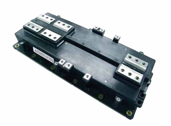
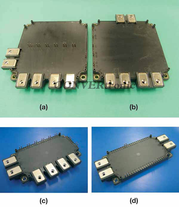
IGBT modules are generally designed in different sizes to meet space and cost requirements. Furthermore, the IGBT module range comprises many different package elements, such as package type, base, terminals, insulators, and power chips. The NX series utilizes unified packages and common assembly processes, enabling us to offer a wide range of circuit modules, not only individual modules but also 2-in-1, 7-in-1, and CIB (converter-inverter-brake) configurations. We can also offer other unique configurations as required for certain applications. Some package types are shown in Figure 1. Flexibility is offered for both circuit configuration and terminal design.
Chip Technologies:
IGBT Chip Progress.
Figure 2 shows the FOM, which indicates the IGBT performance transition. The FOM is defined as the chip current density (JC), divided by the product of the saturation voltage (VCE(sat)) and the power loss at turn-off (Eoff) per impulse per unit current in inductive switching at Tj = 125 °C. CSTBT™ technology has a better FOM than trench IGBT technology. The FOM of Mitsubishi's sixth-generation IGBT is 30% higher than that of the fifth generation.
 Sixth Generation IGBT
The sixth generation IGBT chip is based on advanced CSTBT™ technology. Figure 3 compares the cross-sectional views of the 6th generation IGBT with the conventional 5th generation IGBT. Both types share a common concept in CSTBT™ technology by utilizing the Carrier Stored (CS) effect. As a first step in the development of the sixth generation IGBT, the wafer structure was modified from NPT (Non Punch Through) to LPT (Light Punch Through) technology through the development of a thin wafer process technology [2]. Second, the cell design was optimized to improve the VCE(sat) - Esw(off) trade-off ratio.
Narrowing the cell groove and optimizing the CS layer doping enhance the CS effect in this layer [3]. The result is a drastic improvement in the VCE(sat)-Esw(off) trade-off ratio, as shown in Figure 4. Another important consideration is that the IGBT's power loss performance has a trade-off relationship with the SCSOA (Short Circuit Safety Area). Figure 5 shows the SCSOA data obtained for the sixth generation of IGBT chips. The CS layer optimization and cell design provide more than 10 ms of short-circuit withstand capability without sacrificing the IGBT's power loss performance.
New FWDi Design
Figure 6 shows the structure of a new flyback diode (FWDi) design compared to a conventional FWDi. As shown in Figure 7, the thin-wafer process technology contributes to improving the trade-off between the forward voltage VF and the switching loss recovery Esw(rec).


'


 On-Switch Behavior:
Reducing the dv/dt ratio during power-up switching typically helps suppress EMI noise radiated by the equipment. Generally, by controlling the gate speed of an external circuit, the on-switch dv/dt can be reduced; otherwise, reducing dv/dt will increase the on-switch loss (Esw(on)) in the IGBT chip. Figure 8 shows the trade-off relationship between Esw(on) and dv/dt. The switching speed can be controlled by changing the gate resistance. The Esw(on) of 6th generation IGBT chips is 20% lower than that of conventional IGBTs at the point where dv/dt = 7.5 kV/ms, which we assume as a hypothetical user condition.
The smoothness of the inverse recovery value in the FWDi and the inverse transfer capacity (Cres) in the IGBT contribute to improving the Esw(on)-dv/dt trade-off ratio. This result implies that 6th generation IGBTs have a wider selection range and good power loss control capability as a function of noise level.
Turn-Off Behavior:
At the moment of turn-off, there are multiple electron pair holes and free electrons in the N-layer, so the collector current cannot stop abruptly. The collector current gradually decreases over a period of time, which depends on the electron lifetime. Incidentally, the 6th generation IGBT improved the tail current through optimization of the LPT structure. Figure 9 shows the waveforms during turn-off. The tail current of the 6th generation IGBT chips is lower than that of the 5th generation. A lower tail current leads to lower Esw(off) losses.
 Power Loss Performance:
Power loss in general PWM inverter applications has been estimated for both 5th and 6th generation IGBT modules (see Figure 10) for a 1200 V/150 A nominal module used at full load capacity of 30 kW at 400 VAC. The gate resistance was selected in each device so that the dv/dt ratio yielded the same value (7.5 kV/ms). The total power loss in an IGBT/FWDi chip consists of switching loss and static loss. Our calculations show that the losses of the sixth generation IGBT module are 20% lower than those of the conventional module.
Thermal Simulation:
The thermal simulation of the NX series is shown in Figure 11. The simulation was performed assuming a 1200 V/1000 A NX series device, packaged in a 2-in-1 package, with a 400 V input, running a 185 kW inverter at full load. The junction temperature (Tj) for a 6th generation IGBT module is on average 25 °C lower than that of conventional IGBTs. The junction temperature of the new FWDi is on average 21 °C lower than that of conventional FWD. Therefore, it is possible to reduce the space, weight, and cost of the cooling system.
Reliability Limits:
In many cases, the lifespan of an IGBT module is dominated by thermal fatigue at the junction during intermittent operation. Figure 12 shows the lifespan of the latest NX series module compared to the older module (H series). The NX series, with its 6th generation IGBTs, has the same lifespan as the current NX series and is better than the H series. Incidentally, an increase in the maximum junction temperature limit, Tj, is also seen as a requirement when considering the design of new power equipment. The NX series, with its 6th generation IGBTs, allows operation at a maximum temperature limit, Tj, of 175 °C. The NX series has been tested under two operating conditions (Tj(max) = 125 °C and Tj(max) = 175 °C). At Tj(max)=175 °C, the 6th generation IGBT shows a lifetime performance between Tj(max)=125 °C of the current NX series and that of the H series (for Tj(max)=125 °C).
 Conclusions:
With the development of the sixth-generation IGBT chip and a new FWDi, the Mitsubishi NX series of IGBT modules will result in improved power losses for power applications. For the IGBT module user, this will mean greater system efficiency. Furthermore, the NX series will offer flexible packaging and improved device characteristics, expanding its application range. The new NX series has great potential for the development of future power systems.
Author: Nishiyama Taketo, Yuji Miyazaki. Works for power devices, Mitsubishi Electric Corporation, Japan.
Bibliography
[1] Manabu Matsumoto et al. “The Development of new IGBT Module with the Unified Package parts” PCIM CHINA 2007.
[2] Takahashi Tetsuo, et al. “CSTBTTM (III as the next generation IGBT” ISPSD 2008.
[3] Satoh Katsumi, et al. “New chip design technology for next generation power module” PCIM Europe 2008.