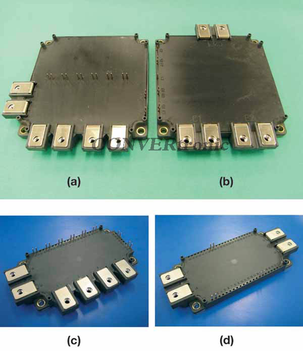
Semiconductor chips are arranged to increase the module's cooling capacity, and a substrate-directly insulated aluminum baseplate is used to enhance thermal cycling capabilities. To achieve better thermal contact between the baseplate and the cooler in a device with such a large base area, the baseplate is divided into multiple sections. The package used for the 2400A/1200V dual IGBT module is also used for the 1800A/1700V dual module.
Introduction
Our conventional IGBT module series, MPD (Mega Power Dual), which includes a 1400A/1200V dual device, was developed to enable better design in high-power industrial equipment. However, with the recent expansion of renewable energy generation systems such as wind turbines and photovoltaic panels, there is a demand for larger power systems. To meet this market demand in a simple way, a new 2500A/1200V dual IGBT module has been developed.
Structure
and Terminal Layout:
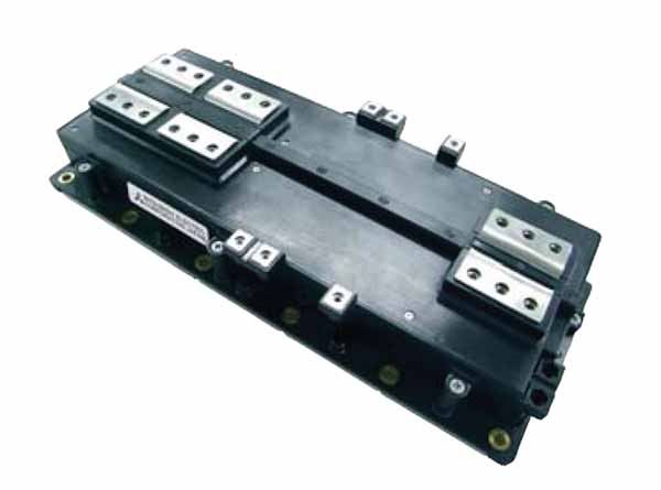
An image of this module is shown in Figure 1. The package length is approximately twice its width. The main P and N terminals are located on one side, and the AC terminal is on the opposite side of the package for more convenient inverter design. The signal terminals are located in the middle of the package, allowing for simple mounting of the driver directly on top of the module. This terminal layout also allows for simple wiring when the driver is separate from the module.


Base Plate Structure:
As the base plate area increases, achieving a tight fit between the base and the cooler becomes challenging. To address this, separate base sections are used for this module. The module housing consists of two parts of varying height to withstand bending stress due to the different base sections. This structure allows for independent testing of each base section. Existing testing equipment, typically designed for testing smaller devices, can be used for this purpose.
The total power loss in a module of this size can exceed 5 kW at maximum power in an inverter application. For such high power losses, liquid cooling is commonly used, and a value of 5000 W/m²K is typically required for liquid cooling in such an application. In liquid cooling systems, the housing temperature changes much more rapidly than in air-cooled systems, making thermal cycling and heat dissipation capabilities critical.
A module will require approximately 400 cm² @ DTc = 25K water cooling under a 5000 W/m²K condition. The chosen base size of our new 2500A/1200V dual module is sufficient for this thermal radiation capacity. However, liquid cooling causes a significant change in the case temperature, thus necessitating an increase in the module's thermal cycling capacity.


To achieve this, an aluminum base plate is bonded directly to the substrate (Figure 5). This structure eliminates the solder layer between the base and the ceramic insulation, a well-known weak point in a conventional module structure after thermal cycling (Figure 4). This solder layer is subject to degradation from temperature cycling stress, resulting in an increase in thermal resistance Rth(x) over the module's lifetime. The thermal resistance of a copper base with a conventional structure and a base with an aluminum structure are compared by simulation and shown in Figures 4 and 5.
Figures 6 and 7 show the simulation results for the thermal resistance of the copper and aluminum bases, respectively.
The thermal resistance values for both types are almost identical, even though aluminum has a lower thermal conductivity than copper. This is a direct result of eliminating the thin, conductive solder layer.


Chip Design:
The chip has been designed to increase cooling capacity when using liquid coolant. The necessary distance between chips, to suppress mutual thermal interference, has been verified through simulation. Figure 8 shows the structure of this simulation. Figure 9 shows the simulation results for the temperature difference between the chip and water at 200 W/chip. The distance between the chips in this module is approximately 30 mm. The results show that this distance is sufficient for liquid cooling.
For optimal cooling performance, the liquid cooling tubing should be positioned directly below the chips.
Therefore, the mounting holes on the motherboard have been chosen to avoid any interference between the tubing and the mounting holes, as shown in Figure 10.


Terminal Structure:
A package with lower inductance is needed when the module's rated current increases. However, if a higher rated current is required, the package becomes larger, so the length of the internal wiring tends to be longer, resulting in an increase in internal inductance. One way to reduce inductance by length is to increase the width of the laminated bus bar inside the module, but this width is limited by the physical space within the module. To achieve a bus bar with lower inductance, a four-layer laminate is used. This structure allows for a reduction in the concentration of current density on the bus and reduces the current density separation ratio for each terminal contact. The inductance value is confirmed by simulation. To ensure the inductance simulation software matches the theory, the simulated value is compared with a calculated value, which is determined using the theoretical equation for a simple structure. Figure 11 shows the simple structure.


µrxµ0x (d / W) xL
• µr = 1
• µ0 = 4šx10^-7
• d: parallel sheet distance.
• W: forward direction distance of the track (width)
• L: parallel direction distance of the current track (length)
The two results are similar. This simulation is therefore a good method for examining the structure. In order to achieve a small bus bar with low internal inductance, a four-layer laminated bus bar is used in this package. Figure 12 shows a bus bar structure.
The target value for the laminated bus bar inductance is 3 nH or less. To achieve this value, two board structures 50 mm wide or more are required. The height of the housing must be 50 mm or less if the package's transformation resistance is taken into account. Therefore, two-sheet structures cannot be used. In our simulation, the best parallel-sheet structure is modeled. The simulation value for the four-sheet parallel structure is 2.59 nH at 1 MHz. This result means that a four-sheet parallel structure is the most suitable solution for this module.


Reducing the module's internal inductance will also improve the balance of how the total current is distributed among each chip. Since L2 is small compared to L1 and L3, the difference in input voltage between each chip is small, thus improving the current balance between the chips.
Module Inductance
Characteristics
Figure 15 shows the inductance simulation structure for the module. To reject the influence of any external wiring, a wide laminated bus is connected to the terminals.
The simulation result for the total inductance inside the module is 5.18 nH from P to N at 1 MHz. This result is lower than the initial target value. Figure 17 shows the test circuit to confirm the inductance of the internal package. The switching device (CM1400DU-24NF) is switching under the 1500 A condition as a di/dt generator. The device under test (DUT) is connected in series, and the voltage spike caused by di/dt is measured between the P and N terminals of the DUT. The inductance of the DUT package is calculated using the waveforms shown in Figure 16.
The inductance of the package within this module is obtained through the following calculations:
di / dt: 9,375 [A / ns]
Vpn (the voltage generated between P and N): 52 [V]
VCE (sat): 1.37 [V] @ Ic = 500A
(VPN-VCE(sat)x2) / (di / dt) = 5.25nH


The same result is obtained with the simulation, achieving the target value.
Characteristics of the Sixth Generation Chips (1200V)
Figure 18 shows the cross-sectional view of the 6th generation IGBT and the 5th generation IGBT.
The trade-off between VCE(sat) and Eoff for our 6th generation IGBTs is reduced by 0.7 V compared to our 5th generation IGBTs at the same Eoff level. Figure 19 shows a comparison of the results of a sample loss calculation for the same dv/dt conditions. This shows that the total loss in an inverter operation for our 6th generation IGBT is calculated to be 25% lower than that of our 5th generation IGBT module under fixed dv/dt conditions.
Features of the Sixth Generation Chips (1700V)
The same package has also been applied to the newly developed 1800A/1700V dual IGBT module. Therefore, we briefly present the characteristics of our 6th generation 1700V IGBT. Figure 20 shows the VCE(sat) - Eoff trade-off. The VCE(sat) - Eoff trade-off is reduced by approximately 0.35V compared to our 5th generation at the same Eoff level. Figure 21 shows the turn-on losses with respect to dv/dt. The turn-on loss has been improved by 25% compared to our 5th generation at the same dv/dt (10kV/ms).
Conclusion:
A new 2500A/1200V dual IGBT module for industrial use has been introduced. Low internal package inductance has been achieved through the use of a 4-layer main internal bus. The chip design has also been optimized for liquid cooling. For improved thermal contact resistance with the heatsink, the base is composed of several parallel sections. Direct bonding between the ceramic substrate and the aluminum base is used to enhance thermal cycling capability. Improved loss performance is achieved using sixth-generation IGBTs and FWDi chips. The same package has also been applied to the 1800A/1700V dual IGBT module, and other module ranges are being considered, utilizing the same standardized base section, thus enabling a good cost-performance ratio.
Authors: Ayumi Maruta, Mitsuharu Tabata. Mechanisms for Power Sources, Mitsubishi Electric Corporation, Japan.
Bibliography
[1] Junji Yamada: Next Generation High Power Dual IGBT Module with CSTBT Chip and New Package Concept, PCIM 2002.
[2] Tetsuo Takashi: CSTBTTM(III) as the next generation IGBT, ISPSD2008-May, pp. 72-75.
[3] Katsumi Satoh: New chip design technology for next generation power module, PCIM 08.