This driver works in conjunction with external power devices such as DrMOS (MOSFET and driver), power blocks, as well as discrete N-channel MOSFETs and gate drivers, facilitating flexible configuration design. Up to eight phases with two ICs can be used in parallel and synchronized to minimize input and output filtering when very high currents of up to 260A are required. Applications include power distribution systems and industrial systems, FPGAs, DSPs, processor power supplies, and ASICs.
The LTC7851/1-1's internal current distribution loop equalizes the current between phases when used in parallel, facilitating precise current distribution between phases across multiple ICs in both steady-state and transient conditions. It operates with a VCC supply between 3V and 5.5V, is designed for buck conversion with an input voltage between 3V and 27V, and produces one to four outputs between 0.6V and 5V. The device's voltage-controlled architecture allows for the selection of a fixed operating frequency between 250 kHz and 2.25 MHz, or it can be synchronized with an external clock over the same range. The output current is sensed by monitoring the voltage drop across the output inductor (DCR) for maximum efficiency, or by using a low-value sensing resistor. Internal differential amplifiers provide remote sensing of the actual output voltage for all VOUT and ground terminals for high-precision regulation.
The LTC7851-1 is similar to the LTC7851 but has a lower current-sensing amplifier gain and is ideal for power transmission applications using DrMOS with internal current sensing. Additional features for each phase include current monitoring, adjustable current limiting, soft-start or programmable tracking, and a power-good output voltage signal. Furthermore, it maintains a voltage reference accuracy of ±0.75% over an operating temperature range of -20°C to 85°C.
The LTC7851-1 is offered in a 5mm x 9mm 58-pin QFN package and is available from stock.





- Details
- Category: Integrated Circuits
Multi-phase quad output DC/DC buck driver operates with DrMos or power blocks to provide up to 260A
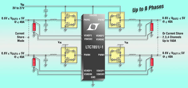 Linear Technology presents the LTC7851/-1, a synchronous quad-output DC/DC buck controller with precise inter-phase current distribution and differential output voltage detection.




Print Magazine

Annual subscription price:
You will receive all 10 editions that are published each year.
social networks
Popular News Electronics



Spanish electronics magazine. Printed for over 25 years.
Spain - Madrid - All rights reserved © Convertronic Professional Spanish Electronics Magazine.