 Toshiba Electronics Europe is set to announce the development of its next generation of its deep trench superjunction (SJ) semiconductor technology for high-efficiency power MOSFETs.
Devices based on the new DTMOS V process operate with lower EMI noise and reduced ON resistance (RDS(ON)), compared to the earlier DTMOS IV MOSFETs.
Similar to the previous DTMOS IV semiconductor technology, DTMOS V is based on a unique epitaxial process involving a deep trench etching process followed by P-type epitaxial growth. The deep trench etching process results in narrower cell pitches and lower RDS(ON) compared to more conventional planar processes. Toshiba's deep trench process enables improved RDS(ON) thermal coefficients for MOSFETs compared to conventional superjunction MOSFETs using the multiple epitaxial growth process.
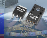
With DTMOS V, Toshiba has been able to reduce the RDS(ON) of the TK290P60Y DPAK by up to 17% compared to the lower RDS(ON) available from the TK12P60W DTMOS IV MOSFET. The company has also further optimized the trade-off between switching performance and EMI noise.
DTMOS V MOSFETs will simplify design and improve performance in power conversion applications, including switched-mode power supplies, power factor correction (PFC) designs, LED lighting, and other AC/DC applications. The first MOSFETs based on the fifth-generation process will offer 600V and 650V and will be supplied in DPAK (TO-252) and TO-220SIS (intelligent isolation) packages. The highest ON resistance ratings will range from 0.29 Ω to 0.56 Ω.