
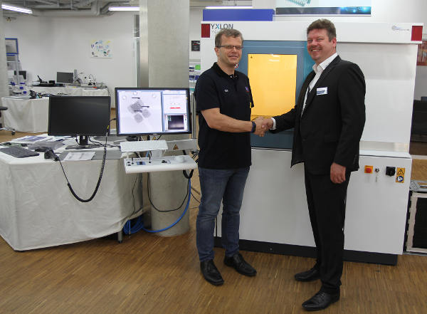
Voids have a significant impact on the quality of solder joints, which is why automotive manufacturers are applying increasingly higher acceptance limits for modules. However, not all manufacturers possess the necessary technical equipment. For this reason, the Rehm Technology Center offers its customers the opportunity to thoroughly inspect their circuit boards and optimize their processes. A variety of SMD and analytical equipment, supported by professional assistance, is used for fault management. With the new YXLON Cheetah µHD radiographic analysis system, solder joints can be inspected in great detail. This tool enables high-resolution, uninterrupted, real-time, and micro-focused radiographic analysis of parts and modules, circuit boards, electronic and mechanical modules, sensors, MEMS and MOEMS, as well as electromechanical components and connectors. To achieve this, it combines several innovative advances: detailed focused radiographic technology, high power target, a state-of-the-art, long-life, precisely calibrated flat detector, and a vibration-damped manipulator, in addition to eHDR inspection, micro-CT and microlaminography.
“Radiographic images help us, among other things, to assess weld quality and void percentage. Based on this, we can discuss with the customer the possibility of implementing other vacuum processes and optimizing existing processes. Furthermore, this system offers a full range of state-of-the-art radiographic inspection capabilities, including laminography and computed tomography. The result is a wide array of manual and automated analysis possibilities, such as distance measurements, BGA and weld point analysis, as well as inspections at the weld level of modules, conductive materials, substrates, and much more. The results obtained form the basis for proper process optimization. In this regard, we place particular value on the system's simplicity, flexibility, and, above all, accuracy,” says Helmut Öttl, Director of Process Development/Application at Rehm.
Laminography allows us to generate precise tomography scans of large or double-sided plates, as well as multi-layered semiconductor components. But computed tomography (CT) offers, above all, a three-dimensional view of the analyzed parts, simplifying the analysis of internal structures, dimensional measurements, and must-have comparisons of CAD data. Furthermore, CT provides valuable information for the production process and allows for detailed visualization of minute structures and components. "The YXLON Cheetah microfocused radiography analysis system perfectly meets customer requirements: precision, flexibility, ease of use, and speed. For modern manufacturers, this is the only way to address the increasing complexity of electrical and electronic components that require detailed analysis," emphasizes Thorsten Rother, Market Manager at YXLON.