We believe that the GaN market will far exceed that figure as early as 2025.
While quantifying the numbers can be challenging, the growth is undeniable. Over the past 18 months, we've witnessed the rise of GaN as the preferred technology for smart device adapters and chargers. Leading brands like Apple, Anker, OPPO, and Xiaomi are basing their new, stylish chargers on GaN thanks to the efficiency and high-performance power delivery offered by GaN switches.
These same advantages (higher power, significantly higher efficiency, smaller size) are also very useful in many other markets. Sectors such as automotive, data centers, LED drivers, renewable energy, consumer audio, and mobile phones are beginning to recognize that GaN's superior switching performance is also suitable for their applications.
 What's driving this tsunami of GaN applications? First, the devices must be robust and reliable. Second, they must be easy to use. Third, the devices must be available in large quantities to ensure security of supply, something especially relevant given the much-publicized semiconductor shortage crisis. Finally, and perhaps most importantly (and truth be told, probably the main reason why customers are reluctant to adopt new technologies), there's the price: the industry isn't willing to pay much more for GaN.
Innoscience was founded in December 2015 to address all of these aspects. Let's start with an unequivocal statement: Innoscience has the world's largest facility for manufacturing 8-inch GaN-on-Si (gallium nitride on silicon) wafers. We'll come back to that later.
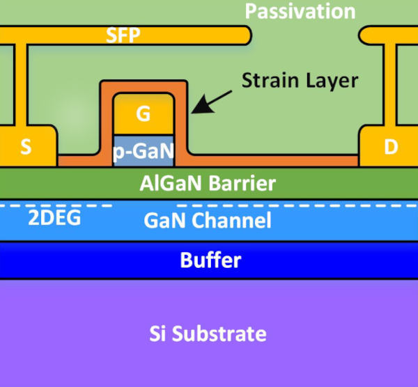
Innoscience has developed its proprietary InnoGaN™ technology. GaN is inherently a normally active process, but systems and application engineers required it to be normally inactive. This caused some problems for early adopters as GaN control became more complex. Companies have addressed this issue in various ways, primarily by using a cascode-type stacked technique with a discrete driver or one integrated into the same package. While these techniques offer an interesting solution, they suffer from some cost and package size limitations. Innoscience induces the growth of a GaN positive layer on top of the AlGaN barrier, thus forming a Schottky contact with the GaN positive layer, resulting in normally inactive operation in enrichment mode.
Innoscience's InnoGaN technology offers another significant advantage: a very low RDS(on). The company has developed a voltage-enrichment layer technology that involves depositing a specific layer after defining the gate stack. The stress modulation induced by the voltage-enrichment layer generates greater piezoelectric polarization, which in turn increases the 2DEG density and thus reduces the lamellar resistance by 66% compared to a device without a voltage layer. Thanks to this innovation, Innoscience's GaN-on-Si enrichment-mode HEMTs are characterized by a very low on-delay specific resistance.
 When addressing performance and ease of use, Innoscience observed that the factor preventing GaN from becoming the dominant technology for power switching was volume. Device availability (or the lack thereof) raises concerns about security of supply; conversely, the availability of large quantities allows for economies of scale and lower prices. For this reason, Innoscience decided to focus solely on producing 8-inch wafers from the company's inception, while other manufacturers offer 6-inch and even 4-inch processes.
Innoscience currently has a capacity of 10,000 8-inch wafers per month, which will increase to 14,000 8-inch wafers per month by the end of this year and to 70,000 8-inch wafers per month by 2025. Furthermore, production throughput is very high because Innoscience uses state-of-the-art manufacturing technology (proven in silicon devices) and has optimized epitaxial and wafer processing. Since Innoscience is a fully integrated company that controls all phases of manufacturing, from device design and epitaxial and wafer processing to failure and reliability analysis (i.e., the entire GaN-on-Si production process), it is able to guarantee high quality. Innoscience's first factory (there is another one operational) has already obtained ISO 9001 certification and IATF 16949:2016 certification for automotive use, and Innoscience's GaN HEMTs meet the JEDEC standard. Innoscience also conducts more advanced reliability testing.
Therefore, to summarize, Innoscience has commercialized reliable, high-performance GaN devices for both low-voltage (30-150V) and high-voltage (650V) applications. Unlike the rest of the semiconductor and electronics markets in general, the company does not suffer from supply shortages. Its products are readily available, and its prices are in line with market demand. Stay tuned for the surge of applications that are about to emerge.
AUTHOR: Denis Marcon, General Manager of Sales and Marketing in Europe and the USA, Innoscience