
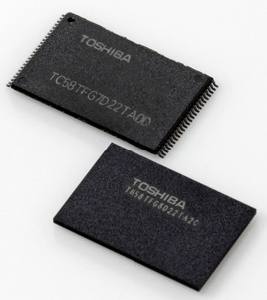
 Shipping samples of products using the new process technology begins today.
BiCS is based on a cutting-edge 48-layer stacking process, which improves write/erase endurance reliability and increases write speed, making it suitable for use in various applications, primarily solid-state drives (SSDs).
Since making the world's first announcement on 3D flash memory technology[3], Toshiba has continued development toward optimizing mass production. To meet market growth in 2016 and beyond, Toshiba is actively promoting migration to 3D flash memory by rolling out a product portfolio that emphasizes high-capacity applications, such as SSDs.
The company is also preparing for mass production at the new Fab2 facility at Yokkaichi Operations, its NAND flash memory production plant. Fab2 is under construction and will be completed in the first half of 2016 to meet the growing demand for flash memory.
Further information or quote
Notes:
[1] As of March 26, 2015. Toshiba survey.
[2] A vertically stacked structure of flash memory cells from a silicon plane with a significant density improvement over conventional NAND flash memory, where the cells are arranged in a flat direction on a silicon plane.
[3] Toshiba presentation, June 12, 2007.