 The proprietary low-noise buck-boost topology performs the function of two separate switched-mode regulators, resulting in savings in size, cost, and complexity. The LTC3110 operates in two modes: standby and charge. In standby mode, the device maintains a supply voltage (VSYS) of 1.71V to 5.25V, supplied by the energy stored in the supercapacitor. Furthermore, the supercapacitor storage input (VCAP) is characterized by a wide operating range between 5.5V and as low as 0.1V. This ensures the utilization of all the energy stored in the supercapacitor, allowing for extended standby time or reduced storage capacitor size. Additionally, in charge mode, when the main power supply is active, the LTC3110 can autonomously or by user command reverse the direction of power flow, using the regulated system voltage to charge and balance the supercapacitors. VCAP is efficiently charged to above or below VSYS using a PWM buck-boost modulator. The device also includes a programmable average current limit in charging mode up to 2A with +/-2% accuracy, thus preventing overload of the system power supply and minimizing capacitor recharge time.
The LTC3110's active load balancing eliminates the constant current draw of external resistive dissipation ballasts, ensuring proper charging even with unequal capacitors and less frequent charging cycles. Programmable peak capacitor voltage regulation actively balances and limits the voltage across each capacitor in the series stack to half the programmed value, ensuring reliable operation as capacitors age and develop varying capacitances. Low-RDS(ON) and low-gate-load synchronous switches provide high-efficiency conversion 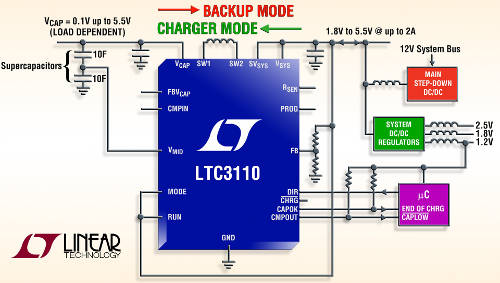 to minimize charging time for storage devices. The LTC3110 is ideal for safe charging and protecting large capacitors in backup power applications such as servers and RAID systems, and battery- or capacitor-backed RF systems.
The LTC3110's input current limit and maximum capacitor voltage can be programmed using a resistor. The average input current is precisely controlled within a programmable range of 0.125A to 2A. Burst Mode® operation can be selected with a pin and improves efficiency with small loads, reducing quiescent current to as low as 40µA and turn-off current to less than 1µA. Other features of the LTC3110 include a high switching frequency of 1.2MHz to minimize the size of external components, thermal overload protection, two voltage monitors for direction and end-of-load control, and a general-purpose comparator with an open-collector output for connection to a microcontroller or microprocessor.
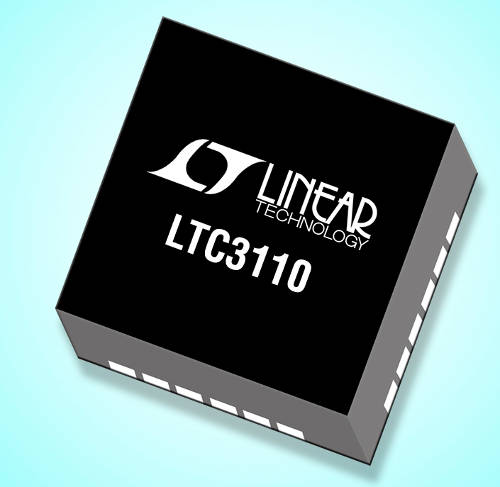
The LTC3110 is supplied in compact, thermally enhanced 24-terminal TSSOP and 24-terminal QFN packages (4mm x 4mm); both with Grade E and I operation between -40°C and 125°C, and up to 150°C for the high-reliability Grade H.
Main features of the LTC3110
• VCAP operating range: 0.1V to 5.5V
• VSYS operating range: 1.71V to 5.25V
• Automatic switching between charging and standby modes
• Precise, programmable charging input current limit of ±2% between 125mA and 2A
• Standby supply voltage accuracy: ±1%
• Automatic standby capacitor balancing
• Fixed switching frequency of 1.2MHz
• Burst Mode® operation: 40μA IQ
• Programmable multifunction comparator with open-collector output
• Open-collector outputs to indicate operating direction and charging end
• Low-profile TSSOP-24 and QFN-24 packages (4mm x 4mm)