They will also find applications in renewable energy, such as photovoltaic (PV) inverters and bidirectional DC-DC converters, such as those used for charging electric vehicles (EVs).
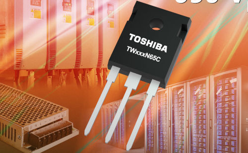
The new TW015N65C, TW027N65C, TW048N65C, TW083N65C and TW107N65C are based on Toshiba's advanced third-generation SiC process, which optimizes the
cellular structures used in second-generation devices.
As a result of this advancement, the FoM calculated as the product of the drain-source resistance (RDS(on)) and the drain-gate load (Qg) to represent static and dynamic losses has improved by approximately 80%.
Like the previous devices, the new third-generation MOSFETs include an integrated SiC Schottky barrier with a low forward voltage (VF) of -1.35V (typical) to suppress RDS(on) jitter, thereby improving reliability.
The new devices are capable of handling currents (ID) up to 100A and feature RDS(on) values as low as 15mΩ. All devices are housed in an industry-standard TO-247 package.