 Unlike Cholesky, where equations (1) to (6) are implemented as a single nested four-level loop, the QR solver employs a single finite state machine (FSM) to cycle through the four main operations: finding the square of a vector's magnitude in equation (2), the dot product of two vectors in equation (4), the subtraction of a dot product of a vector in equation (6), and the dot product in equation (7) to find the vector d. The NestedLoop block in the DSP Builder Advanced Blockset is used in all phases of the FSM to generate all the event control signals for the data path.
The common processing block in the four operations mentioned above is the dot product generator. To improve performance, vector processing is used to calculate the dot product. Similar to the Cholesky design, the vector size is a compile-time parameter. To reuse this generator in the four states of the FSM, a data multiplexer is used at the input and is controlled by the FSM's event handler. The multiplexer selects the correct inputs for the dot product generator in each FSM state. The details of the dot product generator and the floating-point accumulator are similar to those in the Cholesky design and are therefore not included here.
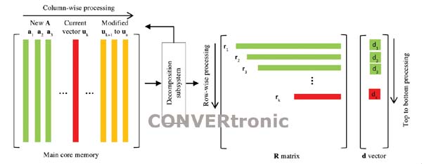
The memory required for QR decomposition is optimized by reusing the main kernel memory block that initially contains matrix A and input vector b. Processing takes place column-wise, from left to right, in kernel memory. Once a column is completed and no longer needed, it is overwritten with the corresponding column of a new matrix. When the old array A decomposes, the original contents of this memory block are replaced by a new array, thus maintaining the array's end-to-end processing capacity without pauses.
In the first two states of the FSM, the elements of the matrix R are generated element by element in row direction, starting with the diagonal element for each row. In the subtraction state of the FSM, the columns of the matrix A in main memory are recursively updated and replaced with the partially computed vectors. For example, in column k, all columns k+1 an are updated in memory by subtracting the scaled version of from each of the columns k+1 to n. This process recursively computes the vectors uk+1 to un and is a more efficient version of equation (6) for hardware implementation. Processing column-directed in the fourth state of the FSM, each newly computed uk is multiplied by the input vector b to generate a single element dk of the column vector d. The Q matrix is not explicitly generated, but its orthogonal columns, uk, are generated and used in later phases of the FSM. These columns are then overwritten in the corresponding column, ak, of the new matrix in the next FSM cycle. Figure 5 shows the memory organization and processing sequence of the QR decomposition subsystem.
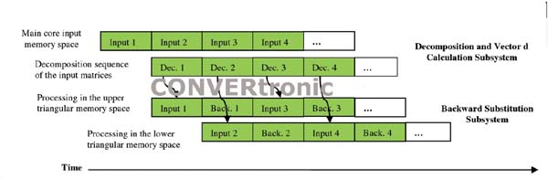
The outputs of the first subsystem are the matrix R and the column vector d. The matrix R is an upper triangular matrix and is generated column-wise from left to right, as indicated by equations (3) and (4). A ping-pong triangular memory structure is applied. While the upper triangular section is being processed in the back-substitution subsystem, the lower triangular section is filled by the decomposition subsystem, and vice versa. The column vector d is added to the matrix R and is generated column-wise from top to bottom. The output of back-substitution is the solution vector x of the linear equations Ax = b.
The QR solver can be implemented in a multichannel format similar to the Cholesky solver to improve utilization, reduce latency, and increase design performance. The performance improvement is primarily due to the effective reduction of floating-point accumulator latency.
3. Design Flow and Toolkit
Evaluation Methodology
For this evaluation, Altera provided BDTI with implementations of the Cholesky and QR solvers created using the DSP Builder Advanced Blockset. Altera provided BDTI engineers with a PC pre-installed with Altera's tools and MathWorks. BDTI engineers then examined, simulated, and synthesized the Altera designs within the Simulink environment. The synthesized designs were then applied to two separate devices: the Stratix V and Arria V FPGAs. During this process, BDTI evaluated Altera's design flow and the performance of the two sample designs.
Since the cards used for this evaluation could not generate the stimuli for the sample designs, each design contains a stimulus generation block implemented using DSP Builder Advanced Blockset blocks and compiled with the design of the application under test. To minimize the stimulus block's impact on test design performance and FPGA resource usage, matrix A is generated on the fly by the stimulus block from a much smaller set of random data. This small dataset is generated using m-file scripts in MATLAB, loaded into the stimulus block's memory, and compiled with the design. These MATLAB scripts use the same algorithm as the stimulus block in the test design to generate double-precision floating-point reference data for the solution vector x in order to measure the error level of the Simulink models and designs fed into the FPGAs. In the Cholesky design, this algorithm guarantees a positive Hermitian definition for matrix A, while the design using the QR solver guarantees the creation of a well-conditioned matrix A. Four vector, matrix, and channel size configurations were implemented for the Cholesky solver design: three on the Stratix V FPGA and two on the Arria V device, with one configuration common to both. For the QR solver design, four configurations were implemented on the Stratix V FPGA, and two of these were also implemented on the Arria V device. All configurations were evaluated for FPGA resource utilization, maximum clock frequency, performance, and functional correctness. FPGA design constraints, such as clock frequency, device selection, and speed level, are specified in the Simulink environment.
 Performance and capabilities were evaluated at both the Simulink model and hardware platform levels. The Simulink model for both designs was instrumented to visualize both the forward process and the total number of forward and backward processing cycles, while the Quartus II software provided the maximum frequency (Fmax) achieved for each configuration. Each configuration was then downloaded to the hardware platform, its operating frequency was set to Fmax, and the process was started. The solution vectors (x) of each solver for each configuration were captured and compared with the corresponding double-precision floating-point references generated in MATLAB.
The post-simulation script calculates the difference between the Simulink IEEE 754 single-precision floating-point output and the double-precision floating-point reference vectors generated in MATLAB. Similarly, the script calculates the difference between the output captured from the hardware simulations and the double-precision floating-point references generated in MATLAB.
Evaluation of the Simulink toolkit
is based on, and therefore requires, the MATLAB environment. In the Simulink environment, the evaluated designs use blocks from the DSP Builder Advanced Blockset, which is a separate blockset from the DSP Builder standard library. The DSP Builder Advanced Blockset is geared toward a block-based implementation of DSP algorithms and data paths, and uses a higher level of abstraction than the DSP Builder standard library, which includes more general and elementary blocks. The DSP Builder Advanced Blockset library contains over 50 common trigonometric, arithmetic, and Boolean functions, in addition to the more complex functional blocks for the Fast Fourier Transform (FFT) and FIR filters. Notable additions to Quartus II version 12.0 include its low-latency square root, nested for loop, and customizable floating-point accumulator blocks. Elements of the Standard Blockset and the DSP Builder Advanced Blockset cannot be mixed in a data path structure at the same hierarchy level; only the blocks in the DSP Builder Advanced Blockset support the floating-point compiler. The blocks in the Standard Blockset are not optimized for floating-point processing. Furthermore, while hand-coded HDL import is available for the Standard Blockset, it is not available for the DSP Builder Advanced Blockset because the tool cannot perform HDL-level implementations. In general, the block-based approach to design input is well-suited to DSP algorithms; however, because constructs such as `case` or `switch` are not available in the block library, a text-based approach is more intuitive for control-intensive designs and those involving state machines.
Running a simulation with DSP Builder Advanced Blockset compiles the Simulink model, generates HDL code and constraints for Altera's Quartus II software environment, generates a test bench and script files for the ModelSim environment, and simulates the Simulink model. Simulation times for various configurations ranged from 3 to 28 minutes, depending on the array size, using an Intel Xeon W3550 PC. The Simulink simulation provides detailed resource utilization estimates without requiring the Quartus II software compilation, thus helping the designer quickly determine the necessary device size. When using a hardware development kit, the user must provide the output pin assignment based on the board layout. The user can apply output pin constraints in the supplied .qsf file within the Quartus II software project folder for the design, or use the Quartus II software pin configuration to assign and manage the output pins from the outset.
Tests were performed on the model to evaluate the ease of exploration of the algorithm and the generation of the corresponding HDL. Input parameters, such as the dot product size, matrix size, and data type, were changed in the stimulus block and during simulation execution. In all cases, the correct RTL code was generated within minutes, and the simulation results matched the MATLAB reference.
All configurations were synthesized using Quartus II design software, which can be launched directly from the Simulink environment. A designer can use Quartus II in push-button mode with default or user-selected optimization parameters, or use the Design Space Explorer (DSE) tool. DSE, part of Quartus II, automatically executes multiple router passes using a different seed for each pass. The route with the best clock frequency is saved. This is an automated process that requires no user intervention but takes significantly longer than the push-button method, which with Quartus II took between 1 and 6.5 hours depending on the design size.
The high level of abstraction applied by the DSP Builder Advanced Blockset design flow accelerates the exploration and simulation cycles of the algorithmic space, thus reducing the overall time required to achieve an optimized final design. However, this advantage is not inherent to Simulink in the same way that, for example, data type propagation is. To take advantage of the design space exploration benefits offered by the block-based design method compared to hand-written RTL, the designer must take additional steps when creating the Simulink model. Specifically, the model must be structured to allow exploration of the algorithmic space based on parameters. For the examples analyzed in this article, the models were implemented to allow testing with different matrix sizes, vector sizes, and (in the case of the Cholesky solver) the number of parallel channels. Once a model incorporating this flexibility is created, performance and resource usage estimates can be explored for various design configurations by varying these parameters. It is also necessary to understand the hardware design to achieve good levels of performance and resource utilization, as exemplified by the floating-point accumulator discussed in Section 2 of this article.
Training for the DSP Builder Advanced Blockset design workflow includes 4 hours of lectures delivered by Altera and approximately 10 hours of online seminars and demonstrations. In addition, BDTI spent approximately 90 hours studying the tool and both models in hands-on sessions. The time and effort required to become proficient with the toolkit will depend on the designer's skill and prior knowledge.
An engineer experienced in Simulink block-based design and hardware design will likely find the DSP Builder Advanced Blockset-based method efficient and easy to use. For an FPGA designer with little or no knowledge of MATLAB and Simulink, designing at a higher level of abstraction may represent a new way of thinking and therefore an initial challenge, which can affect the learning curve. Once familiar with the methodology, the designer can achieve significantly faster design cycles than with HDL. They can focus on implementing the algorithm without worrying about hardware design details such as segmentation. Design and verification time is significantly reduced since most of the simulation and functional verification is performed in the Simulink environment. The RTL output from the Simulink build can then be run in ModelSim software for a complete functional simulation.
The learning curve may be less steep for an engineer with prior system-level design knowledge and little to no hardware design experience. While the toolkit integrates hardware compilation, synthesis, routing, and automatic script generation within the Simulink environment and abstracts numerous complex design concepts such as data segmentation and signal vectorization, some hardware knowledge is still necessary to complete an implementation.
(Continued in April)
Author:
By the Berkeley Design Technology, Inc. team. October 2012