The reverse recovery time (Trr) of HSDs is only minimally affected by temperature, ensuring fast switching across a wide temperature range.
The TK5P60W5 (with Id = 4.5A and RDS(on) = 0.99 Ω) is housed in the smallest package in the series, a DPAK (A-252) package, and achieves a typical diode reverse recovery time of 65 ns. Its input capacitance (Ciss)of 370 pF and a QG of only 11.5 nC support efficient switching operation.
The new TK62N60W5 (RDS(on): 0.045 Ω) is the largest MOSFET in the series, housed in a 3-pin TO-247 package, and supports the highest output power of Id = 61.8A. It achieves a typical diode Trr of 17 ns, Ciss of 6500 pF, and QGof of 205 nC.
The DTMOS IV-H chips are manufactured using Toshiba's "Deep Trench" technology, which offers lower ON resistance (R<sub>DS(ON)</sub>) at higher temperatures compared to conventional superjunction MOSFETs. It also offers reduced turn-off switching losses (E<sub>OSS</sub>) compared to previous generations of technology. The combination of smaller increases in R<sub>DS(ON)</sub> at high temperatures and the reduced diode Trr provides greater efficiency and helps designers minimize system size.
Samples of both devices are currently available, with the TK62N60W5 already scheduled to enter mass production, and the TK5P60W5 scheduled to enter mass production in October 2015.





- Details
- Category: Integrated Circuits
DTMOS IV power MOSFETs with integrated high-speed diodes
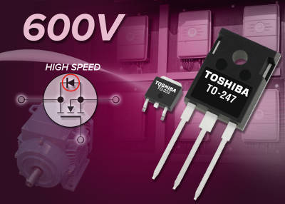 Toshiba Electronics Europe has expanded its range of 600V DTMOS IV MOSFETs with integrated high-speed diodes (HSDs) for use in high-efficiency power supplies and full or partial bridge motor control applications.




Print Magazine

Annual subscription price:
You will receive all 10 editions that are published each year.
social networks
Popular News Electronics



Spanish electronics magazine. Printed for over 25 years.
Spain - Madrid - All rights reserved © Convertronic Professional Spanish Electronics Magazine.