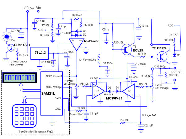
 Analog Circuit (Figure 1)
For specifications of 0-30V and 0-1A, I needed to find components capable of working with a high voltage (< 35V) in the analog section of the design. I chose the MCP6V51, a line of high-voltage operational amplifiers, and the MCP6C02 high-side current sensors, as they met the requirements of my design.
The design is a conventional constant-voltage and constant-current error integration feedback circuit. The selected operational amplifiers, MCP6V51, can handle voltages up to 49V and are notable for their low drift and good DC performance. The resistor values are kept low (10kΩ) and equal at the inverting and non-inverting inputs to minimize any offset error. These resistors, along with the 1µF capacitors (C1, C2), provide an RC filter function to eliminate any residual noise from the digital-to-analog converter (DAC) outputs. The adjusted voltages are supplied by the microcontroller's DACs, from 0 to 3.3V, so the input voltage feedback must be set to this level using R1 and R2.
Regarding current, it is preferably measured on the high-potential side to maintain a common ground and to use the lowest possible current sensing resistance, thus minimizing both voltage drop and power dissipation. The MCP6C02 high-potential current sensor meets these criteria. It can operate at up to 65V and with a gain of 100, allowing for a small current shunt. Since the maximum current expected for this application is 1A, the shunt resistance should be approximately 30mΩ, which would produce a feedback voltage of 30mΩ * 1A * 100 = 3.0V. The resistor is implemented with a copper trace 40mil wide (approximately 1 mm) and about 64 mm long on the printed circuit board (see Figure 3).
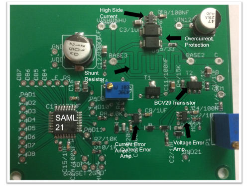
The load on a laboratory power supply can range from an open circuit to a short circuit, so additional protection components are necessary. The 1A general-purpose diodes connected in opposite directions (D1, D2), along with the current-limiting resistor R3, ensure that the differential input voltage of the current-sensing chip remains below the maximum voltage of 1.2V under any conditions. The integrating capacitor (C3) in the current amplifier must be several orders of magnitude larger than the one on the voltage side to compensate for the propagation delay added by the current-sensing amplifier, thus stabilizing the loop. A second channel of the microcontroller's DAC supplies the adjusted voltage (which in turn provides the adjusted current) to the current-error amplifier U2.
The outputs of the two amplifiers are interconnected in a logic OR gate with the small-signal diodes D3 and D4 to drive the Darlington pass transistors at the output. The OR gate determines whether the power supply is in constant voltage or constant current mode.
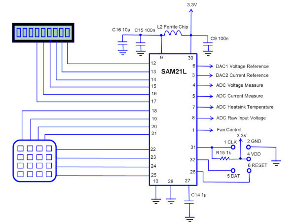 Microcontroller circuit (Figure 2)
The microcontroller controls the keypad and LCD screen, as well as generating the reference voltage levels for the analog control loops, which requires two DAC channels with good resolution. An A/D converter (ADC) will be used to measure various power supply parameters.
The Atmel SAML21 was selected because it has two 12-bit DAC channels complemented by a 12-bit ADC in a small 32-pin TQFP package. The application doesn't require a full 12-bit DAC; however, some additional headroom is advisable since there is a slight loss of precision due to specification and rounding errors when the firmware calculates the values.
firmware
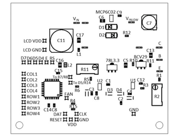
code is written in C, and there are two versions of the driver: one provides basic functions and is called PowerSupplyBasic.c, adjusting and measuring voltage and current; the full version, called PowerSupplyFull.c, also measures the heatsink temperature, switches a fan depending on the heatsink temperature, displays the input voltage and power, and the power dissipated in the pass transistor. These drivers are available in the reference and should be added to a Studio 7 project along with the PowerSupply.h starter file. The program was compiled using Studio 7 IDE (version 7.0.129), and an Atmel ICE was used for programming and debugging. The programming pins on the printed circuit board are not compatible with the standard connector supplied with the programmer, so a new connector must be installed to ensure the pins align with those shown in Figure 2 and with the board layout.
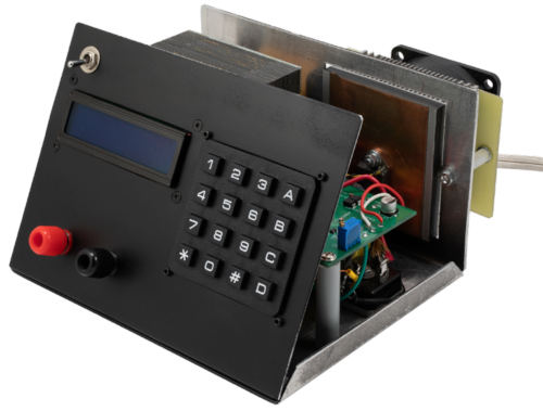 At power-up, the voltage is set to 0 V and the current to 50 mA. The display shows the set voltage and the measured voltage on the first line, and the set current and the measured current on the second line (Figure 5).
If the full version of the driver is installed (as well as the associated hardware as explained below), the auxiliary functions can be displayed.
The main interface works like this: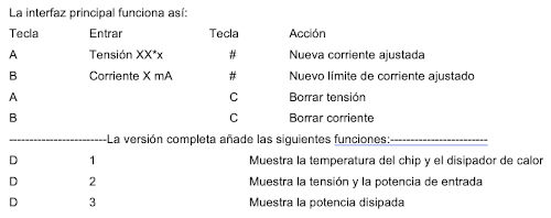
Hardware:
Breakdown voltages for passive surface-mount components are not usually a concern since most circuits operate at low voltages. This application is an exception, and therefore it is important to pay attention to this parameter. Some of the capacitors I used on the printed circuit board are rated at 50V or higher. There are good reasons to use 50V (or higher) ceramic capacitors in all positions if a package of that size is available. The capacitance of ceramic chip capacitors is voltage-dependent; the capacitance decreases as the voltage approaches their maximum operating value.
I've added a separate VDD supply to the L78L3.3 voltage regulator, VinLOW. This regulator has a maximum input voltage of 30V. If your power supply provides a higher voltage, VinLOW must be supplied from a separate, lower-voltage power supply, or a component must be inserted to create a voltage drop between Vin and VinLOW. A resistor or a Zener diode will also work; this circuit draws about 25mA of current, mainly through the LED that illuminates the back of the screen.
If you choose the full version, you must also connect diode D5 to ensure good thermal contact with the pass transistor (TIP140). Resistor R14 provides an approximate constant current of 100µA, so the voltage drop across the diode depends only on temperature, with typical values of 0.7V and -2mV/°C. However, there is significant variability in the absolute voltage level and temperature coefficient (slope) between diodes. Therefore, this parameter must be calibrated separately in the software. The SAML21 incorporates a factory-calibrated temperature module, making it a good starting point.
I opted for an aluminum case, and the complete power supply can be seen in Figure 5.
Variations:
If you only want to build the basic version without the heatsink fan, these components are not needed: T3, R9, R14, R7, R8, D5.
I had a transformer that would provide a rectified voltage of about 40V with no load and a nominal current of 1A. Therefore, I set the maximum regulated voltage to 30V and the maximum current to 1A. The pass transistors should provide a combined voltage of 4-5V between collector and emitter at full load.
If you have a transformer that supplies a lower or higher voltage, you can modify the code that sets the DAC's reference voltage. If the desired voltage change is outside the adjustment range of potentiometer R2, you must change the value of resistor R1 so that the voltage at the inverting input of U1 is lower than the minimum high level of the DAC (VDD – 150mV) for the maximum output voltage of the power supply.
The maximum voltage limit is set by the maximum voltage specified for the operational amplifiers and/or pass transistors. With the selected operational amplifiers, the no-load input voltage must be below 49.5V minus a safety margin. The upper current limit depends on the current the pass transistor can handle. The TIP140 is good for 10A of DC collector current, but it's possible to add pass transistors in parallel (with appropriate current-sharing resistors) to further increase the output current. When current levels are high, the power dissipation will also be high, and this will need to be addressed with an appropriate heatsink design. I combined a heatsink and fan from an old PC motherboard, which works very well for 30W. The base control current will not be a problem, even at the 10A level, since the hFE of the TIP140 is still high.
The smaller Darlington control transistor, the BCV29, is limited to a continuous collector current of 0.5A with an hFEMIN = 4000 at that current level, thus providing a very small load for the operational amplifier, U1. This transistor is soldered to the printed circuit board, and for an application requiring only low current, it is possible to omit the externally mounted TIP140 pass transistor and connect the emitter of the BCV29 directly to the power supply output. This transistor is supplied in an SOT89 package for surface mounting, so the power dissipation will be limited because heat dissipation is minimal. If this option is being considered, pay close attention to the temperature of the BCV29 transistor.
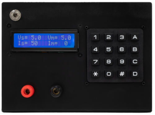 Figure 4. Output screen.
In conclusion,
the microcontroller opens up many opportunities for incorporating functions into this power supply, such as the ability to program a voltage/current curve over time in test and other applications.
The goal of this project was not to design a high-precision commercial power supply but a practical one for my workbench, but it exceeded my expectations.
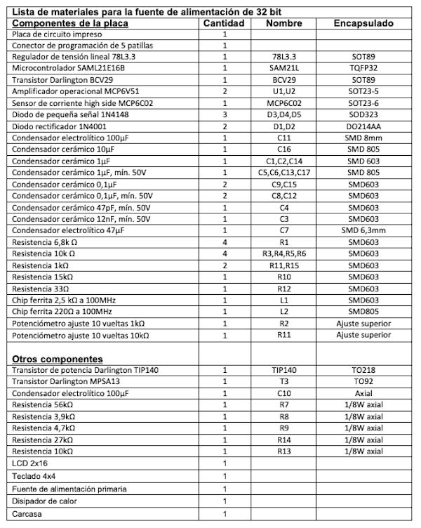
Bill of materials for the 32-bit power supply