 Sources and Effects of Common-Mode Noise in Hybrid Transmission Systems
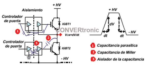
Figure 1 represents a typical block diagram of a hybrid transmission system. When the gate drivers sequentially switch the IGBTs on the high and low-voltage sides, dV/dt noise is generated. For example, a typical transmission system connected to a high voltage of 400VDC with an alternating rise and fall time of 50 ns will generate dV/dt noise of 400V/50ns ~ 8 kV/µs each time the gate driver switches.
Under short-circuit conditions due to faults, the additional overshoot voltage (V = L . di/dt) will be added to the DC rail voltage. This additional overshoot voltage is caused by a large short-circuit transient current (di/dt) flowing through the circuit's stray inductance, L. The gate driver circuit must be able to handle this additional dV/dt noise in order to maintain control and execute the correct protection protocol. Furthermore, the need for a higher DC rail voltage source for larger hybrid vehicles, such as trucks and buses, and the need for a faster switching frequency to reduce driving loss, have increased system requirements regarding dV/dt noise rejection. Typically, a hybrid drive system with a dV/dt noise rejection of 15 kV/µs is essential to maintain overall system performance, reliability, and robustness.
When dV/dt noise couples through parasitic capacitances within the system and causes unwanted voltage transitions, it becomes a serious threat. Over time, it can cause the system to lose control, resulting in false feedback, etc. Although dV/dt noise is undesirable, it naturally exists within the transmission system, as explained earlier. Designers have no choice but to identify and address all possible coupling paths for dV/dt noise. Figure 2 illustrates the possible parasitic capacitances present within a system.
 Solutions
To provide adequate common-mode noise rejection, designers have to deal with the aforementioned parasitic capabilities within the system.
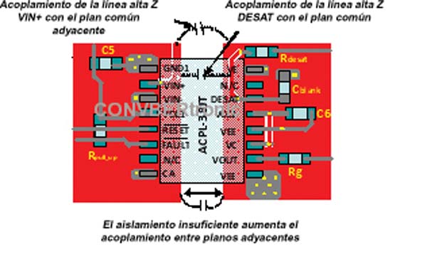
 First, designers should try to minimize external or gate driver circuit parasitic capacitance through efficient design. Maintaining sufficient isolation space between adjacent low- and high-voltage regions of the printed circuit board is essential. Insufficient space will reduce the effectiveness of the isolation and increase parasitic coupling, degrading common-mode noise rejection performance. Furthermore, high-impedance signal lines that are most sensitive to dV/dt noise (i.e., VIN+, VIN, and the DESAT terminals of the ACPL-38JT optocoupler in Figure 3) should be kept as far away as possible from the adjacent isolated region to avoid parasitic coupling. It is always recommended to place bypass capacitors near the driver supply terminals to keep the current supply loop as small as possible and minimize common-mode transient voltage coupling of parasitic inductance. Figure 3 shows a comparison between a dV/dt-sensitive design [3(a)] and a recommended design [3(b)] using the Avago ACPL-38JT optocoupler.
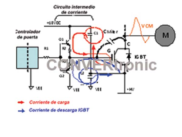
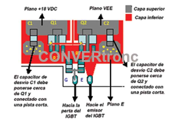
Second, designers must address Miller capacitance coupling. When dV/dt noise couples during switching through the Miller capacitance, it will induce transient noise current. This transient noise current will flow through the existing parasitic inductance along the schematic vias from the IGBT gate to the gate driver, affecting the driver's control voltage. To minimize the effect of dV/dt noise through Miller coupling and to provide cleaner switching waveforms, the designer should keep the IGBT gate's charge and discharge loop as small as possible. An example of a current intermediate circuit for the IGBT is shown in Figure 4(a), and a recommended schematic is shown in Figure 4(b).
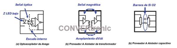
Third, designers must choose the correct isolator to limit or reject common-mode noise coupled through internal parasitic capacitances. Various isolation techniques are commercially available, such as optical isolation (also known as an optocoupler), magnetic isolation (transformer), capacitive isolation, and so on. See Figure 5 for basic internal block diagrams of an optocoupler, a transformer isolator, and a capacitive isolator.

 Among these, the optocoupler is known as one of the most popular and effective isolation techniques for providing high common-mode noise rejection. For example, Avago Technologies optocouplers offer the following advantages for improving common-mode noise rejection:
- Low impedance LED driver. The LED indicator shows the low impedance when illuminated, making it less susceptible to common-mode transient current induced by dV/dt noise. Additionally, the ~80pF LED coupling capacitance helps reject high-frequency common-mode noise.
- Internal shield on the photodiode and IC side of the optocoupler - A transparent shield allows an optical signal to be transmitted while simultaneously helping to redirect common-mode transient current to ground instead of affecting the detector and IC circuit.
Internal shielding is not typically implemented on capacitive and transformer isolators. This is primarily because the internal shield would block the desired magnetic signal coupled into the transformer isolator and the capacitive signal coupled into the capacitive isolator. Without the shield, unwanted dV/dt noise could couple through the same signal channel and affect the control signal.
CMR reference tests of different isolators
 In order to compare the common-mode rejection (CMR) capability of different types of insulators, some gate drivers were selected for internal CMR comparison standard testing. The typical CMR test setup for the insulated gate driver is shown in Figure 6.
 The CMR test results showed that the optocoupler has better CMR (common-mode rejection) than transformer and capacitive isolators. The Avago Technologies gate driver optocoupler (ACPL-38JT) proved capable of withstanding high common-mode transient current without failure and achieved a minimum CMR of 30 kV/µ for both high (CMH) and low (CML) output levels. This performance is significantly better when compared to available transformer and capacitive isolators. A summary of the test results is shown in Table 1.

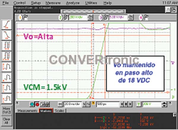 Taking a closer look and comparing the CMH waveforms of the three different isolators, no faults are seen in the CMH waveform of the optocoupler's gate driver. Figure 7 shows that the Avago gate driver optocoupler is able to maintain a high output state with a dV/dt of 67 kV/µs and VCM = 1.5 kV, resulting from the low-impedance LED driver and internal shield, which effectively enhance the gate driver's CMR capabilities. Figure 8 shows that Supplier A's transformer isolator failed the CMH benchmark test, as the gate driver was unable to maintain its output high even when VCM was at 500 V, with a slow rise time of 160 ns (dV/dt ~ 2.5 kV/µs). Similarly, Figure 9 shows that the CMH level of the capacitive insulator from Supplier B drops to less than 15 kV/µs when the VCM is raised to 900 V, and a failure is observed when the VCM is raised to 1 kV and above for the high output test (dV/dt ~ 4.5kV/µs).

 Conclusion:
Hybrid drive systems are subjected to large amounts of dV/dt noise during use in harsh automotive environments. To maintain system reliability and ensure passenger safety, designers must minimize the unforeseen threat of common-mode noise through sound system design and assembly, and by selecting the appropriate isolation device. A door driver optocoupler featuring a low-impedance LED driver and an internal shield offers significant advantages in rejecting high common-mode transition noise.
Author:
Choo Mei Zhen, Avago Technologies.
Author
Choo Mei Zhen works as a technical marketing engineer at Avago Technologies, with responsibilities for application support and design for automotive insulation. Previously, she worked as a
development engineer in electronics at Dyson. She holds a master's degree in electronic engineering from Universiti Teknologi Malaysia.