 The newly developed technology is an Intelligent Motor Timer System (IMTS), a dedicated circuit block that can be integrated into microcontrollers (MCUs) for next-generation electric vehicles (EVs) and hybrid electric vehicles (HEVs). It performs field-oriented control operations (Note 1), which are essential for EV motor control, in as little as 0.8 microseconds (µs), the fastest rate in the world (Note 2). This is less than one-tenth the processing time of the implementation software operation on a CPU running at the same operating frequency. This contributes to the realization of next-generation high-speed EV motors with excellent energy efficiency and inverter systems with high-speed switching performance to power them.
Furthermore, the unique circuit also enables the functional safety support required for the automotive powertrain field.
 With increasingly stringent fuel efficiency requirements in recent years, EVs, EVs, and plug-in hybrid electric vehicles (PHEVs) have come to represent a growing share of the total number of vehicles manufactured. To expand the range of these motorized vehicles, it is necessary to improve the energy efficiency of engine control.
To achieve this, it is important not only to make mechanical improvements to the engines themselves but also to enhance the functions and performance of the electronic control units (ECUs) that manage them. ECUs capable of supporting next-generation EVs, EVs, and PHEVs require advanced functionality and complex control software, resulting in a substantial increase in the processing load placed on the microcontrollers (MCUs) used in these control units. At the same time, automotive MCUs need to minimize the amount of heat they generate to maintain a high level of reliability in high-temperature environments. Therefore, the operating frequency of the MCU's internal circuitry, including the CPU core(s), must be kept relatively low, making it difficult to increase performance.
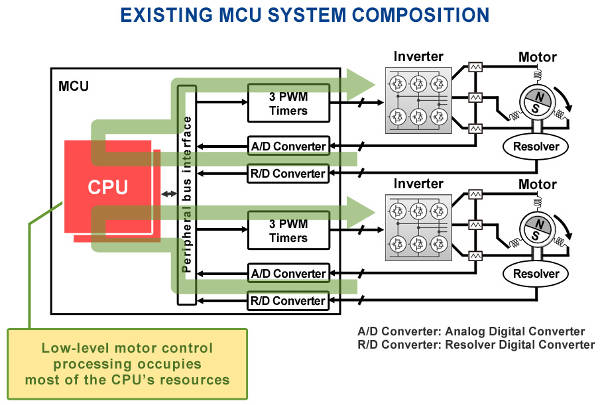
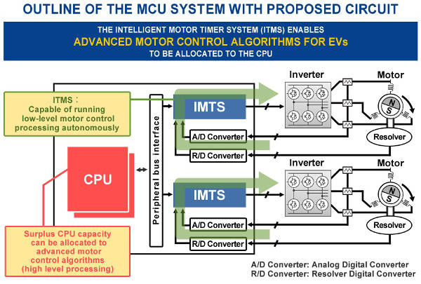
In response to these needs, Renesas implemented the IMTS as a dedicated circuit block for static processes requiring high responsiveness, such as sensor data acquisition, calculation of control values based on that data, and output of those values. The IMTS is CPU-independent and capable of autonomous operation, thus substantially reducing the CPU load on the motor control MCU. The excess CPU capacity can be allocated to advanced motor control algorithms designed to increase the energy efficiency of next-generation EVs, VEHs, and PHEVs.
Key features of the newly developed dedicated motor control circuit technology:
1) Development of a dedicated circuit block for static motor control and circuit technology that enables autonomous operation.
Motor control requires a series of static processing steps involving field-oriented control operations. During each control period, the motor current and angle values are acquired by the MCU's internal timer circuit, and these values determine the control values for the next control period. The resulting PWM output (Note 3) is then generated based on these control values. When multiple motor control types operate simultaneously, the resulting processing load can consume up to approximately 90% of the CPU capacity (Note 4) in a Renesas 40-nanometer (nm) 320 MHz automotive MCU. The newly developed IMTS is a dedicated circuit block for these processing-intensive field-oriented control operations. It is also configured in close conjunction with a dedicated motor control timer circuit, resulting in a system where the processing sequence performed during each control period managed by the timer circuit—from obtaining the current and angle values to the PWM signal output—is carried out autonomously, independent of the CPU.
This means that all the CPU load previously required for the preceding processing is eliminated, and the CPU capacity thus freed up can be allocated to software containing advanced control algorithms designed to increase energy efficiency.
By providing a dedicated circuit for processing field-oriented control operations, IMTS reduces the operation processing time to 0.8 μs, which is less than 1/10th of the CPU-based software implementation. The processing performance of this new technology is sufficient to meet the demands of high-speed switching inverter control (performance example: 100 kilohertz (kHz) switching frequency, 10 μs control period) using power devices made from novel materials such as silicon carbide (SiC), which are on the horizon for the next generation of EV motor control.
2) Development of circuitry technology providing the functional safety required for power control.
Transmission control must ensure functional safety so that if a component fails, the system will detect this and automatically transition to a safe state. This has generally been achieved by using two MCUs to provide system redundancy, or by using one MCU with redundant internal circuitry, which could lead to a relatively high cost.
The developed technology uses an MCU with two CPUs in a dual-core lockstep configuration that regularly monitors the internal operation of the IMTS circuit. This approach keeps costs down while achieving high-speed control and functional safety. Functional safety places a load on the CPU, but in practical use cases, it is estimated to account for only 2.4 percent (Note 5) of the CPU's total processing capacity.
3) Development of circuit technology for flexible error correction of external sensor signals.
To manufacture a high-precision MCU with highly accurate operational processing, it is essential to acquire highly accurate sensor signal values. However, it is impossible to avoid errors from a variety of sources, such as errors caused by the sensor mounting position. The developed IMTS has a configuration that makes it possible to correct errors in real time using user-developed software. Furthermore, the IMTS performs this processing autonomously, so the correction processing does not place a load on the CPU. The corrected sensor signal values are used for engine control operations, resulting in more precise operation and improved energy efficiency when the engine is running.
Renesas is testing a prototype 40nm MCU with built-in flash memory that incorporates these new technologies. It is using a real-world engine drive system to confirm its performance in a real-world setting. Renesas aims to contribute to the development of more energy-efficient ECU systems for EVs, VEHs, and PHEVs by utilizing this dedicated engine control circuitry technology.
Note 1: Field-oriented control operations are a basic type of processing widely used in motor control, in which complex calculations, including trigonometric functions, are used for coordinate conversion to generate DC signals that more closely approximate the designated control values.
Note 2: As of February 7, 2017, based on research by Renesas.
Note 3: PWM stands for pulse-width modulation, the type of pulse signals used to drive an external power device using an MCU.
Note 4: Next-generation systems are expected to require a motor timer control period of 12.5 μs. The calculated value for CPU load assumes that two motor control operations (e.g., for the motors driving the front and rear wheels) occur simultaneously during each control period.
Note 5: The calculated value for CPU load assumes a use case in which faults are detected within the duration of a single rotation when the motor is running at a speed of 100,000 rpm.