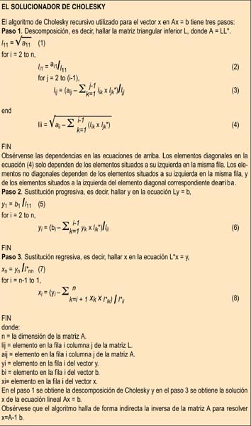
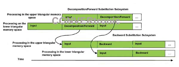
 Since the input matrix is Hermitian and the decomposition generates complex triangular conjugate transpose matrices, memory usage is optimized by loading only the lower triangular half of the input matrix A and overwriting it when generating the lower triangular matrix L. Both subsystems are pipeld and use an input stage and a processing stage to allow processing to take place in one area of memory while the other half is used to load new data. The output of the decomposition and forward substitution stages goes to the input stage of the back substitution, as shown in Figure 2.
The main part of the decomposition consists of the complex dot product generator (also called the vector multiplier), which computes equations (3) and (4). For the Stratix V device, a vector size (VS) of up to 90 complex data elements is used, while for the Arria V device, a vector size of up to 45 complex data elements is implemented. The vector size corresponds to the number of parallel memory reads required to provide the dot product generator with a new set of data for each clock cycle, and thus determines the width and partitioning of the on-chip dual-port memory. For implementation reasons, the storage of an array of a given size is divided into (N/VS) ceiling memory banks, where ceiling (VS) is the ceiling function and N is the array size.
The Cholesky solver design is multi-channel. The maximum number of channels is a compile-time parameter and is limited only by the available memory on the device. Memory partitioning is identical to the single-channel implementation, with the difference that a certain number of copies of the same structure are made.
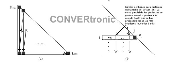
The decomposition is performed element by element, column by column, starting at the top left corner and proceeding vertically in a zigzag pattern, ending at the bottom right corner of the matrix, as shown in Figure 3(a). First, the diagonal element of each column is computed, followed by all the non-diagonal elements below it in the same column, before moving on to the diagonal element at the top of the next column to the right. The event and iteration schedule is controlled by a nested four-level for loop. The outermost loop processes the column; the second loop processes the bank; the third inner loop processes the rows; and the innermost loop processes the different channels. Placing the channel processing as the innermost loop effectively turns the floating-point accumulator into a time-sharing accumulator and better hides its latency. The NestedLoops block in DSP Builder Advanced Blockset integrates up to three nested loops into a single processing block, speeding up implementation and making more efficient use of resources compared to a similar function implemented as three separate for-loop blocks. The block extracts intricate loop control signals, reduces design and debugging time, and makes the loop structure more readable
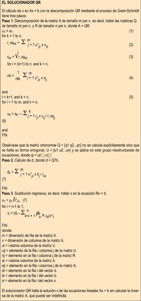 The scalar product generator works with the rows of the matrix and calculates multiplications up to the size of the vector in the sum term of equations (3), (4), and (6) simultaneously in a single cycle. A circular memory structure is used at the input of the scalar product generator in row cycles of the multiple input matrices.
For scalar products shorter than the vector size, unused terms are masked and not included in the sum. For scalar products longer than the vector size, partial sums of the products are calculated and stored within the bank boundaries until all available banks for a given element in the corresponding row are summed for a final sum, as shown in Figure 3(b). The summation of the bank outputs is performed in a single accumulator loop using the floating-point adder block in the DSP Builder Advanced Blockset. The feedback loop has a latency of 13 cycles. By swapping the Banks loop and the Rows loop relative to their traditional software implementation order, and by adding multichannel processing, the floating-point accumulator latency is hidden, improving hardware utilization.
The DSP Builder Advanced Blockset automatically calculates loop delays to address this latency. The tool can be configured to calculate and use the minimum delay by checking the Minimum delay box in the Loop Delay block. Paths that cause identical delays can be assigned an equivalence group number, and the tool will then assign the same delay value to all members of the group. Although not used in the examples evaluated in this article, the DSP Builder Advanced Blockset provides an application-specific floating-point accumulator that the user can customize to optimize its speed and resource requirements by configuring parameters such as the maximum input size and the required accumulation precision. This block allows for single-cycle-per-sample accumulation of a single stream of floating-point numbers at a high clock frequency.
 The second subsystem performs back substitution. This subsystem has its own input and output memory blocks. Like the Cholesky forward substitution subsystem, it is segmented into an input stage and a processing stage. Since the complexity of back substitution is on the order of N² compared to N³ for decomposition, vector processing is not used for the inner product. Instead, a single complex multiplier is used for the inner product, which is sufficient to follow the steps of Cholesky decomposition and the
 forward decomposition subsystem.
Author:
By the Berkeley Design Technology, Inc. team. October 2012
(Continued in March)