

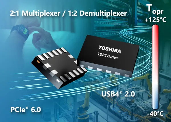
The devices utilize Toshiba's proprietary SOI process (TarfSOI™) to achieve a typical differential bandwidth of -3 dB at 29 GHz for the TDS5B212MX and 34 GHz for the TDS5C212MX. These wide bandwidths reduce signal distortion and improve reliability in high-speed data transmission. Furthermore, both products feature optimized pin designs to enhance high-frequency performance. Specifically, the TDS5C212MX minimizes the signal path length to reduce reflections and transmission losses, further improving high-speed signal integrity.
The devices can be used as 2-input, 1-output multiplexers (Muxes) or 1-input, 2-output demultiplexers (De-Muxes), and support data rates up to 64 GT/s for high-speed differential interfaces, including PCIe® 6.0, USB4® version 2.0, CXL™ 3.x, Thunderbolt™ 5, and DisplayPort™ 2.0. Both products are also backward compatible with interface standards. The devices allow for flexible sharing of a single high-speed interface among multiple devices and dynamic switching of the signal path based on system requirements.
Housed in the XQFN16 package (2.4 mm × 1.6 mm × 0.4 mm), the products are suitable for high-density designs, such as smartphones and wearable devices. Furthermore, they operate within a temperature range of -40 °C to +125 °C, making them ideal for space-constrained industrial applications.