

One emerging answer is the 3-level DC-DC converter architecture, which can offer impressive efficiency gains while reducing bill of materials (BOM) cost and board size.
Why a 3-level DC-DC converter?
A 2-level Buck controller uses two FETs (external or internal) and a single inductor for power transfer. They are called 2-level controllers because the inductor's phase node (V_SW) oscillates between VIN and ground—that is, only two levels. In this topology, the FETs must block the entire VIN voltage when turned off, and the inductor ripple reaches its maximum at a 50% duty cycle.

Figure 1: Typical 2-level DC-DC topology
The three-level (3N) buck converter consists of two additional switches and a flyback capacitor compared to a conventional two-level (2N) buck converter. Switches Q1 and Q4 are phase-shifted, and similarly, Q2 and Q3 are also phase-shifted. The switching node (V_SW) alternates between VIN and VIN/2, or between VIN/2 and ground, hence the name "3 levels"

Figure 2: Typical 3-level CC-CC topology
In steady state, the flyback capacitor maintains VIN/2, which reduces the voltage across the switches. This allows the use of lower-voltage FETs with a better factor of merit, leading to a reduction in conduction and switching losses proportional to V².
This topology also allows the use of a smaller inductor, as the inductor only sees half of VIN. Inductor ripple occurs at twice the FET switching frequency, making the peak-to-peak ripple only a quarter of that of a 2-level converter, resulting in reduced inductor core and DCR losses.
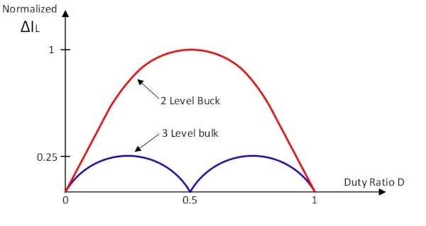
Figure 3: Inductor ripple versus duty cycle for 2- and 3-stage buck converters
Bill of Materials Reduction Opportunities
: By leveraging the improved thermal and electrical efficiency of 3-level designs, engineers can:
- Reduce the size of inductors and capacitors without compromising performance.
- Reduce the number of components by simplifying snubber circuitry and EMI filtering.
- Select MOSFETs with lower voltage ratings, which are more cost-effective and have lower conduction losses.
Real-world application examples:
Multi-port USB-PD chargers.
In high-power USB-PDs (especially EPR >65 W), efficiency and thermal control are critical. A 3-level DC-DC converter can operate at higher switching frequencies without penalty, allowing for smaller magnetic components and faster transient response. Reduced thermal load enables sleeker enclosures without forced ventilation, directly lowering manufacturing and material costs.

Figure 4: Diagram of a multi-port USB-PD charger with 3-level DC-DC
Power Products for Consumers:
In products such as laptops, connectivity stations, and high-end portable audio equipment, board space is often at a premium. A smaller power stage not only reduces the bill of materials cost but also frees up space for additional features, improved aesthetics, or a smaller overall form factor. Featuring an innovative power stage design that incorporates a 3-level switching node and a 2-level switching node via the inductor, this architecture enables buck, buck-boost, or boost modes.
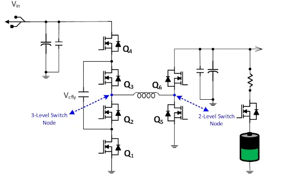
Figure 5: Power consumption product with 3-level DC-DC diagram
Advantages of Voltage Reduction:
Since each component in a 3-level converter experiences less voltage swing, the voltage reduction requirements are less stringent. For example, in a 2-level buck converter that steps down 24 V to 5 V, the high-side MOSFET might see the full 24 V during the off state, requiring a 30 V–40 V device with a higher R_DS(on) and higher cost. In a 3-level topology, the MOSFET receives only about half (≈12 V), allowing the use of a 15 V–30 V MOSFET with a much lower R_DS(on), better switching performance, and lower cost.
This effect extends throughout the design: voltage reduction allows designers to choose from lower-voltage, higher-performance component families, which often have better factor of merit (FOM) and lower conduction and switching losses. The net result is a smaller, cooler, and less expensive power stage.
Advantages Regarding Inductor Size and Efficiency:
Since the ripple current in a 3-level converter is naturally reduced, the required inductor size is also reduced. For example, in a 2-level buck converter that steps down 24 V to 12 V, the inductor must control the complete 24 V to 0 V transition in each cycle. This results in a higher peak-to-peak ripple current, forcing designers to select higher inductance values and physically larger inductors with a larger core volume and copper windings. Larger inductors not only increase cost but also introduce higher DC resistance (DCR), which adds conduction losses and further reduces efficiency.
In a 3-level buck converter, the effective voltage across the inductor is halved because the switching transitions occur between intermediate voltage nodes (approximately 12 V to 0 V or 24 V to 12 V). This reduces ripple current by almost 50%, allowing for a smaller inductance value to achieve the same current ripple. Smaller inductors with lower DCR directly lead to reduced conduction losses, faster transient response, and a more compact design. At the same time, lower ripple reduces the output capacitor voltage and improves system reliability. The combined result is higher efficiency, a smaller footprint, and a lower overall system cost, making the 3-level topology particularly attractive for high-current and space-constrained applications.
System-level impact
The switch to a 3-tier CC-CC architecture is not just a component-level change, but has system-wide implications that can translate into quantifiable benefits throughout the product design
• Reduced thermal design requirements
: Because the 3-level topology reduces switching and conduction losses, less heat is generated in the power stage. For example, in a 200W USB-PD charger, heat dissipation could be reduced by 1–2W compared to a two-level design. This can allow you to replace a bulky aluminum heatsink with a smaller stamped metal piece or even eliminate it entirely, eliminating the need for thermal pads or heat pipes and reducing bill of materials costs and assembly complexity.
• Smaller PCB area dedicated to power conversion:
With lower losses and voltage, inductors and capacitors can be physically smaller. In a typical laptop adapter, the power stage area could be reduced by 20 to 30%, freeing up valuable board space for additional ports, wireless charging coils, or an improved mechanical design. Smaller components also allow for higher component density, making it easier to meet case size or weight targets.
• Greater efficiency translates into lower operating costs for the end user.
In high-volume consumer devices, even a 0.5–1% efficiency gain results in tangible energy savings over the product's lifetime. For example, a 240W, 3-level USB-PD charger with 95% efficiency will waste 12W less energy per day than a 2-level design with 93% efficiency when used at full load for eight hours, reducing electricity costs and heat buildup for the end user. This is especially important in enterprise or data center environments, where dozens or hundreds of such units may be deployed.
Conclusion:
The 3-level DC-DC converter offers an attractive way to maximize value in power delivery systems. By reducing bill of materials costs, decreasing component size, and simplifying thermal management, this topology allows designers to deliver high-performance, cost-optimized products that meet the demands of modern applications. As USB-PD and other high-power markets continue to grow, the 3-level approach will become an increasingly attractive option for engineers focused on both performance and cost-effectiveness.
By Alex Zhou, Director of Product Marketing at Renesas