
Robust and resilient SiC MOSFETs.
It can be argued that SiC MOSFETs constitute the most critical link in a power system chain. Therefore, they must demonstrate robustness in several areas where they have been vulnerable. Like silicon MOSFETs, they also face the problem of extrinsic defects such as impurities, charge states, and other material defects near the oxide-semiconductor junction, which cause various types of device instabilities and degradation mechanisms. Eliminating these risks requires that production SiC MOSFETs demonstrate a stable threshold voltage, a reliable gate oxide, a robust intrinsic structural diode, and avalanche resistance. Each attribute must be validated through qualification testing, as parameter stability and lifetime can vary greatly depending on the supplier.
To verify the stability of the threshold voltage (Vth) of a SiC MOSFET, a high-temperature positive (p-HTGB) and negative (n-HTGB) gate bias is typically applied to stress a statistically significant number of devices, and the Vth before and after the stress test is simply compared. For example, p-HTGB and n-HTGB were applied to separate assemblies of sixty-four 1200 V SiC MOSFETs for 1000 hours. The average change observed in Vth was +59.6 millivolts after
p-HTGB and -22.8 millivolts after n-HTGB. With this level of stability, developers have a predictable threshold voltage from which they can make more stringent and longer-term design decisions.
High-reliability gate oxides are paramount in all applications, especially those requiring a long lifespan. To determine the reliability of the gate oxide in SiC MOSFETs, load-to-breakdown (QBD) measurements were performed on three 1200 V SiC MOSFET assemblies. All observed failures were intrinsic, indicating a high level of process maturity. Time failure rates (FIT) and mean time between failures (MTTF) were calculated for a larger number of devices, specifically 192. For p-HTGB, these values were 20 and 5,618 years, respectively; for n-HTGB, the results obtained were 93 and 1,233 years. These results should be encouraging for end users, as they are consistent with time-dependent dielectric breakdown (TDDB) reports provided by various suppliers.
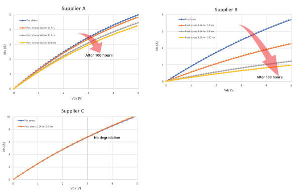
The phenomenon of bipolar degradation in SiC pn junctions has been extensively studied. If structural diode degradation occurs in a SiC MOSFET, increases in both forward resistance and voltage drop across the diode during current switching would be observed (manifested by a downward trend in the third-quadrant output characteristics). Fortunately, SiC MOSFET materials have evolved, and the defect density in pre-existing crystals has decreased in production materials. Even so, it is necessary to evaluate SiC MOSFETs from each supplier. Ohio State University recently compared structural diode degradation after 100 hours of stress at maximum rated current (VGS = -5 V) in 1200 V SiC MOSFETs from several suppliers and observed substantial differences in forward resistance after the stress phase. Only Supplier C showed no degradation (Figure 1). Supplementary third-quadrant data on the same devices corroborated the presence (or absence, for Supplier C) of structural diode degradation.
 Figure 1. The third quadrant data show that the Supplier C SiC MOSFET was the only one that did not experience structural diode degradation. Source: Dr. Anant Agarwal and Dr. Minseok Kang, Ohio State University.
Another important parameter is avalanche resistance, which is performed using unclamped inductive switching (UIS). The MOSFET is subjected to an electrical overload while OFF, forcing the current to generate an avalanche at the periphery of the semiconductor die since the MOS channel is not enriched.
This differs from a short-circuit resistance test, in which the MOSFET is ON and the current is distributed more evenly across the active area of the device. To better simulate real-world operating conditions, SiC MOSFETs are subjected to repetitive UIS pulses (R-UIS); parameter stability and oxide integrity are compared before and after 100,000 repetitive pulses at two-thirds of the rated current (per MIL-STD-750). VBR, Vth and VF of the structural diode are not affected by R-UIS, indicating its excellent avalanche resistance.
Low-Inductance Power Packages:
Once confidence in the SiC MOSFET is established, the next piece of a complete SiC system is an optimized power package. An effective multi-chip module package should allow designers to take advantage of SiC rather than limit it.
Numerous requirements must be considered. Since the SiC MOSFET semiconductor die is relatively small, many of them must be connected in parallel to achieve low on-resistance. Furthermore, the parallel MOSFET semiconductor die must switch synchronously and share current evenly, which means ensuring symmetry and low inductance in the semiconductor die interconnection schemes.
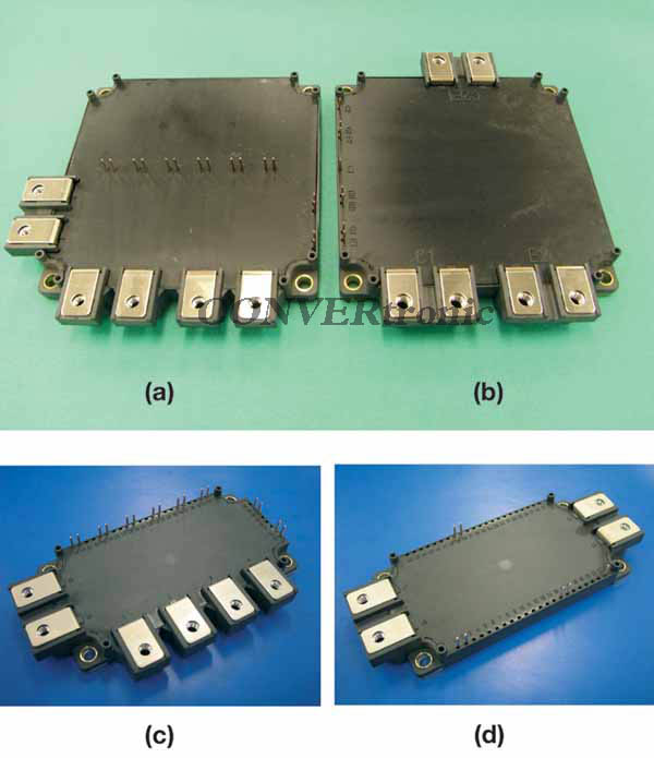
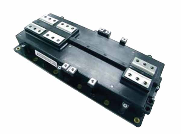
An example of this is Microchip's SP6LI package, which adds only 2.9 nH of parasitic inductance to the power loop, compared to more than 20 nH of parasitic inductance in standard module packages. The power loop inductance is reduced by establishing the DC link connections on busbars configured in a flat line. The substrate connections are distributed symmetrically and are as close as possible to the semiconductor die. For the gate-source loop, independent series gate resistor slots are used for each of the available slots on the semiconductor die at the high/low side switching positions to optimize timing and current sharing. The independent gate resistors reduce parasitic inductance introduced into the gate-source loop, provide protection against catastrophic tripping, and minimize switching losses.
Intelligent and Flexible Gate Driver Technology:
A third element required for a complete SiC system is control. Again, the ability of SiC MOSFETs to switch quickly means that a non-optimized system is at risk of failure due to EMI and voltage transient spikes. New gate driver technology is needed that allows the designer to manipulate the switching dynamics and achieve an optimal balance. In addition, the gate driver must provide fast detection and response to signal spikes since SiC MOSFETs are characterized by shorter endurance times than most silicon IGBTs.
A patented technique called augmented switching has made it possible for the most advanced digital gate driver solutions to pause at a user-defined intermediate VGS for a desired duration to discharge the Miller capacitance before switching to VGS OFF (see Figure 2). This contrasts with traditional methods that take VGS directly from ON to OFF, thus offering the designer no way to circumvent other, less avoidable system problems, such as parasitic inductance in the cable used to connect the load. In fact, an extraordinary balance between surge protection and efficiency can be achieved by introducing small modifications to the augmented switching profile (VGS levels and dwell time).
 Figure 2: A digital gate driver using the augmented switching method greatly facilitates the identification of optimal design points and their evaluation.
Figure 3 shows turn-off waveforms using two enhanced switching profiles and a 1200 V SiC MOSFET module in a D3 package (106 mm x 62 mm x 31 mm). It can be seen that selecting a lower intermediate VGS reduces switching losses when efficiency is a priority, while a higher VGS attenuates VDS peaks and smooths the oscillations of all three waveforms. 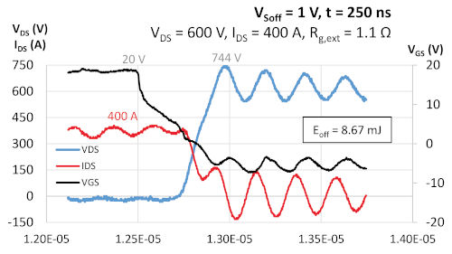 Thanks to the supplied software configuration tool, gate driver settings can be precisely configured at all stages of development with just a click of the mouse, unlike the hours spent using a soldering iron.
Figure 3. Turn-off waveforms showing the effect of enhanced switching on a SiC MOSFET module.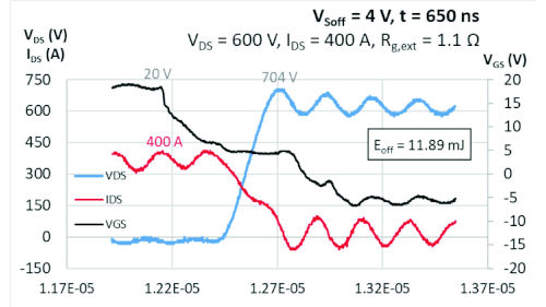
Digital gate drivers can also enhance the level of intelligence. For example, they can be used to provide a completely different turn-off profile in the event of a fault, thus better ensuring safe operation. The addition of enhanced switching methods to short-circuit protection reinforces the use of low Rg, in addition to guiding the MOSFET through a smoother, more controlled transition to OFF with a lower probability of avalanche breakdown. Further configurable features include real-time diagnostic measurements such as DC link voltage and temperature monitoring.
As power electronics evolves from silicon IGBTs to SiC MOSFETs, it relies more on component suppliers to provide the critical elements needed to create complete system solutions. This translates into a SiC MOSFET with proven robustness, a very low inductance power package, and a new class of smart gate drivers designed for easy optimization. All of these are essential for streamlining SiC design from initial evaluation to field deployment.
Author: Kevin Speer, Microchip Technology