Chip/substrate sintered bonds are achieved using special silver particles that, under certain conditions, produce sintered bonds resulting in a reliable connection between the parts. Figure 1 shows the silver particles before and after the sintering process. It is important to note that each of these particles is surrounded by a layer of a special material. The bonding process is simple, requiring only a sufficient number of particles to achieve the desired thickness of the bonding layer and applying the appropriate temperature and pressure for a specific period of time. The result is a very stable bond. However, this basic process needs refinement for industrial application.
In recent years, efforts have focused on the industrialization of this technology. A paste has been developed for use as a starting material in sintering. Furthermore, the necessary tools have been developed to sinter multi-chip ceramic substrates (DCBs) in a 5" x 7" format. The press used in the sintering process has been designed to accommodate different loading pressures depending on the sintering process.
Furthermore, the personnel responsible for the process have been trained, and continuous improvement measures have been implemented.
The contact bond strength achieved with the sintered layer between the chips and the substrate is exceptionally high. Sintered joints demonstrate high resistance to load cycles in reliability tests. Another advantage of sintering technology is the significantly greater accuracy, on the order of 50 µm, in the position of the chips relative to the substrate. In comparison, current soldering technology only achieves a positional accuracy of 400 µm.
Considering the thickness of the sintered layer, it is four to five times thinner than the soldered layer and has four times better thermal conductivity. The result is that the sintered joint exhibits excellent thermal properties. Sintered layers also perform better under load cycles because the melting point of the silver material used in sintering is four times higher than the melting point of the filler material used in the soldering process (see Table 1). The high-temperature stability of the sintered joint indicates that the joint does not deteriorate over time.
Application of Sintering Technology:
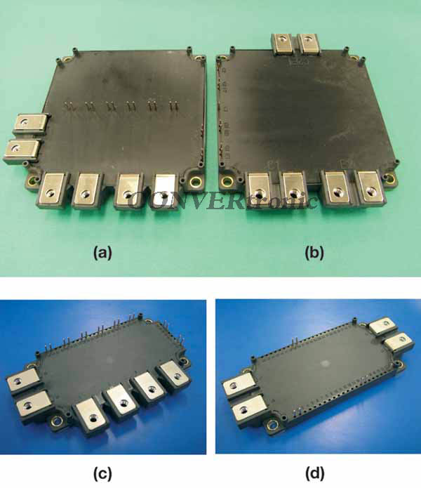
Sintering technology has been employed in SKiM® IGBT modules, used in applications ranging from 22 kW to 150 kW. SKiM® has a thermal cycling resistance up to five times greater than conventional modules with copper soles and solder. Instead of soldering the ceramic substrate, necessary for insulating the module, to the copper sole, the latter has been eliminated by using pressure contact technology when attaching the module to the heatsink (see Figure 3). Pressure is applied at numerous points positioned close to each chip, ensuring uniform pressure distribution across the entire surface of the ceramic substrate. Eliminating the copper sole results in improved thermal cycling performance and lower thermal resistance. Figure 3 shows a cross-section of the module housing, the pressure contact system, and the spring contacts for the control connections.
The elimination of all soldered connections makes the SKiM module family the first 100% solderless module available on the market. The combination of sintering technology, pressure contact technology, and a copper-solder-free design ensures five times the thermal cycling capacity of soldered modules with copper soles.
Over the past 15 years, permissible chip operating temperatures have steadily increased. Currently, modules incorporating the latest chip technology, such as IGBT4/CAL4, can operate at maximum temperatures of up to 175°C. In the future, the use of silicon carbide will present greater challenges in achieving stable junctions resistant to thermal cycling, as the operating temperature for silicon carbide-based components can reach up to 300°C.
This is why the sintering technology developed by Semikron is perfectly suited to these high operating temperature ranges. This is because the melting point of the sintered junction is 961°C, approximately 740°C higher than that of the soldered junction commonly used today.
This stability of the junction at high temperatures prevents degradation. Various reliability and life tests have demonstrated the robustness of the sintered junction.
Over time, the application areas for power semiconductors have changed dramatically. In the past, semiconductor modules were only used in accessible locations, mounted inside cabinets where the environment was highly controlled.
Today, semiconductor modules are used in mobile applications, for example, in vehicles with extreme environmental conditions, temperatures exceeding 110°C, etc. The current challenge is ensuring that the semiconductor module can operate reliably under these harsh conditions.
The Future of Sintering:
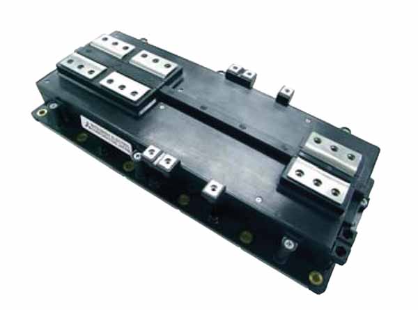
The sintering technology developed by SEMIKRON is a key technology that enables the manufacture of more powerful, reliable power modules with a longer lifespan. The same principles applied in the manufacture of the SKiM module – elimination of the copper sole, pressure contact system, and sintering technology – have been applied to the development of the 4th generation SKiiP smart power module, used in wind and solar power generation, bus traction, subways, and other applications.
The benefits of sintering technology also apply to the 4th generation SKiiP: five times greater thermal cycling capacity than conventional modules, stable bond between the chip and the ceramic substrate, and twice the load cycle capacity of standard modules.
Author:
Christian Göbl, Head of New Technologies, SEMIKRON
More information or a quote